

On Printed Circuit Boards (PCBs) made by Rush PCB, the copper weight of a trace bears a direct relationship to the current it can carry. The current carrying capacity of the trace depends primarily on the cross-sectional area of the trace and its length, the amount of time for which the current flows, and the temperature rise on the trace. To some extent, the current carrying capacity also matters whether the trace is buried in one of the inner layers of a multi-layered board, or exposed on its outer layers. Other factors complicating the issue of calculating the maximum current carrying capacity of a trace are the presence of components, pads, and vias on it.
Defining Copper Thickness
Rush PCB defines the default copper thickness on their PCBs in ounce (oz). A 1 oz thickness of copper signifies 1 oz by weight of copper spread evenly across one square foot area, resulting in a copper layer of thickness of 1.37 mils or 0.0347 mm. Most other PCB manufacturers also follow this default copper weight of 1 oz. Typically, a 0.5 oz copper is generally considered to be insufficient and a thickness of 2 oz is most often an overkill.
However, for applications where the current handled by a board may not be adequately handled by a 1 oz thickness, the design engineer can exercise one of two choices. He/she may specify a higher copper weight, or increase the width of the trace.
Copper Thickness Vs. Width
The manufacturing process presently followed for a PCB ensures that all traces on a layer are of the same thickness. Therefore, specifying a higher copper weight for a trace translates into all traces on the layer being thicker, whatever the current passing through them. On average, as only a few traces on a PCB carry higher current, making all traces thicker for the sake of only a few results in a more expensive PCB. Therefore, selectively increasing the width of a specific trace to allow it to carry higher current is more economical for the design.
Defining Minimum Spacing
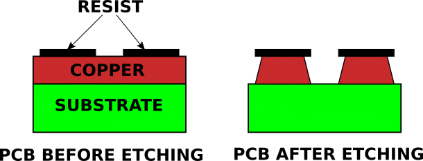
Another aspect that Rush PCB follows while manufacturing PCBs is to make the minimum spacing between traces and the copper weight interdependent. This follows from the fact that the resist protects the copper trace only from the top during the etching process. As the etching of unwanted copper progresses, partial etching also takes place on the sides of the traces. That makes the final cross-sectional shape of a trace almost always a trapezoid, and thicker traces therefore requiring more space between them. Refer Fig.1.
Rush PCB maintains minimal spacing based on PCB copper weight, as follows:
| Copper Weight (oz) | Minimum Space mils (mm) |
| 0.5 | 3 (0.076) |
| 1.0 | 3.5 (0.089) |
| 2.0 | 8 (0.203) |
| 3.0 | 10 (0.254) |
| 4.0 | 14 (0.355) |
Note: the above numbers are indicative only, and may change depending on design and application.
Also Read: DIFFERENT STACKUPS FOR HDI PCBS
If the application calls for a current carrying capacity higher than 4 oz, Rush PCB recommends doubling a layer rather than increasing the copper weight further. Furthermore, fabricating heavy copper on the outer layers of a PCB can be a problem, as the etching process results in a trapezoidal cross-section for a trace (Fig 1). This may mean the SMT pad is actually thinner than the designer intended, and may result in component placement difficulties or to weak solder joints. Moreover, multiple coats of solder mask may be required to protect heavy copper traces.
Copper Width and Current Carrying Capacity
The above discussion leads to the conclusion that the temperature rise allowed and the copper weight of the trace are not enough information to decide its current carrying capacity—other factors such as number of pads, vias, and components also matter, as does the position of the trace, whether it is buried or exposed.
For instance, if the trace has several pads and vias positioned along its length, it is likely to be able to carry a significantly lower amount of current as compared to what any simple tin-plated trace of similar dimensions can, since the pads and vias act as constrictions increasing the electrical resistance of the trace, thereby raising its temperature considerably with a lower value of current. While calculating the current carrying capacity of a trace, designers need to consider such factors.
For such situations, Rush PCB has two solutions. First, increase the trace width if possible—this being the simplest and best solution. However, this may not be always possible, hence the second solution. Open the solder mask on the trace that is getting hot, and print solder paste onto it. Once reflow soldering process completes, solder will cover the entire trace, increasing its cross-sectional area, thereby increasing its current carrying capacity.
For even higher current applications, Rush PCB recommends using multiple planes stitched together with as many vias as possible. Here, the vias divide the current into multiple paths, and the heating along the plane reduces.
The Time Factor
Current flowing through a trace heats it up because of the power dissipated in the trace on account of its internal resistance. The heat raises the temperature of the trace, and enough heat can melt the trace, that is, convert it from solid copper to molten metal. Two time periods are involved here—one to raise the temperature of the trace from ambient to the melting point, and two, the time to actually melt the trace. The second time period is the heat of fusion.
As the trace starts to heat up, it also cools by conduction into the board material, convection into air, and radiation away from the trace. With the heating effect matching the cooling effects, the temperature may stabilize. However, if the heating effect is greater than the cooling, the trace temperature rises further, until the trace reaches its melting point.
As the trace starts to melt, current continues to flow through the liquid copper. However, as molten copper has a lower thermal and electrical conductivity compared to solid copper, the situation creates an explosive run-away condition, often resulting in current interruption as the liquid path separates, as a result of explosive splattering.
If a trace fuses on a PCB, it must not be repaired to put the PCB back into service. A fused trace is a destructive failure, and the board must be removed from service, as the heat from the temperature of fusing may have caused hidden potential problems in the components and the PCB material around that area. Even if it is tempting to design a PCB trace to work as a fuse, this can only be a one-time event—preferably use a fusing component as a replaceable fuse.
Calculating Current Carrying Capacity of PCB Trace
Although several equations exist for calculating current carrying capacity of a PCB trace, the actual practice is tedious when attempted manually, and prone to errors. Rush PCB recommends using the PCB Trace Calculator from UltraCAD. The calculator solves for a wide range of width and thickness of traces.
Rush PCB also refers to standards IPC-2221 and IPC-2222, which are guidelines for trace widths versus their current carrying capacity. For instance, IPC-2221 recommendations for PCB track widths for 1 oz copper weight and 10°C temperature rise are:
| Current (A) | Track Width mil (mm) |
| 1 | 10 (0.25) |
| 2 | 30 (0.76) |
| 3 | 50 (1.27) |
| 4 | 80 (2.03) |
| 5 | 110 (2.79) |
| 6 | 150 (3.81) |
| 7 | 180 (4.57) |
| 8 | 220 (5.59) |
| 9 | 260 (6.60) |
| 10 | 300 (7.62) |
However, one still needs to factor in the various other conditions listed above to reach an effective value for practical use.
Conclusion
The above discussion assumes the current flow through the trace is in steady-state. However, this may not always be the case, and current flow may instead be pulsing. For pulsing currents with a fast-enough repetition rate compared to the thermal time constant of the PCB, Rush PCB recommends using the RMS value of the current for calculations


