

The electronics industry is presently using thinner printed circuit boards (PCBs) and smaller SMT electronic components than they did earlier. The trend comes from increasing customer demands for smaller form factor for electronic devices. According to Rush PCB, the use of thin multi-layer PCBs of less than 40 mils (1 mm) and very small SMT components is also leading to issues of warpage in the assembly process. Warpage impacts the assembly yield, as it affects all aspects of the process.
For instance, PCBs with excessive warpage affect the quality of paste printing during the solder paste printing process. It also affects the formation of solder joints during the reflow soldering process—leading to SMT assembly defects.
Rush PCB presents solutions addressing the PCB warpage issue. We share the results of detailed studies on PCB design, reflow pallet design, and methods of controlling and containing PCB warpage. We recommend changes in PCB design and controls in the assembly process to reduce the impact of PCB warpage, thereby providing improvements in margin for the board assembly process.
What is PCB Warpage?
Ideally, when kept on a flat reference surface, all parts of the PCB should be in contact with the surface. Due to various stresses, this does not happen, and some parts of the PCB do not touch the surface. While some parts of the PCB may bend upwards, other parts may bend downwards, representing positive and negative curvature. Moreover, the bend may be along one or both the axes of the board, or along one or both diagonals. It is also possible for the board to develop a twist. All these are PCB warpage.

What Causes PCBs to Warp?
A copper clad board is typically an electroplated copper film on a substrate. There are two primary factors affecting warpage of this combination. The first factor is the built-in stress on the copper film that causes the board to warp at room temperature under no thermal process. The second factor is the mismatch of the coefficient of thermal expansion (CTE) between the copper layer and the substrate, and this is a dominant factor during temperature changes, such as during reflow.
When fabricators stack individually etched copper clad boards together to form multi-layered PCBs, the process introduces additional factors causing warpage. The copper density on each layer being different, causes differing amounts of stress in each layer, leading to complex warpage patterns.
Fabricators often place PCBs in a panel for improving the assembly efficiency. Panelization uses rails and outriggers to facilitate handling the panel through different stages of assembly. After assembly, operators remove the outrigger, and separate the PCBs by de-paneling them. Copper density in the outrigger area, compared to that of the board area is another factor that affects warpage.
Problems with PCB Warpage
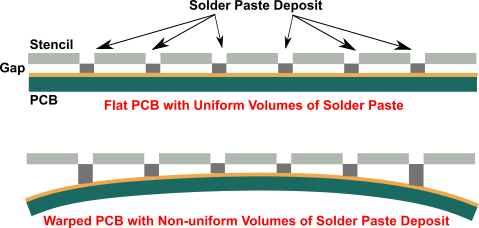
Solder Paste Printing through Stencil: Ideally, there should be a minimum gap between the stencil and the PCB surface, and the gap must be uniform all over. This ensures the solder paste deposit on the PCB is of the correct volume.
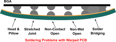
For a warped PCB, some parts of the PCB will be closer to the stencil and other parts farther away relative to the optimum distance. Solder paste deposits on the closer parts of the PCB will have a lower height, hence lower volume. Deposits on the parts with a larger gap will have a greater height and therefore, greater volume of solder. The net result is a non-uniform solder paste deposit, resulting in excess solder for some components, and inadequate solder for some others during reflow. This can lead to problems such as stretched joints, open joints, solder bridges, and head & pillow joints during reflow.
Reflow Soldering: A warped PCB gets worse with increase in temperature—its warpage increases. A PCB may be on the threshold of acceptance at room temperature during the solder paste printing process. However, during reflow, if the warpage increases, it can affect soldering under close-pitch ICs such as BGAs.
Preventing PCB Warpage
At room temperature and elevated temperatures both, PCB warpage impacts board assembly. However, there is lack of industry specification for PCB warpage.
Although the IPC-A-610E standard specifies maximum warpage for incoming PCBs at room temperatures, this is not adequate when the temperature rises, as warpage increases with temperature.
According to IPC-TM-650, the maximum bow and twist for an SMT PCB must not exceed 0.75%. However, according to Rush PCB, limiting it to 0.5% is a better choice.
Balance Copper across PCB layers: At the design stage, designers must consider copper balancing across all layers around the central core to prevent board warpage. Balancing the copper distribution helps to minimize CTE mismatch both at room and at elevated temperatures. However, design constraints may not allow perfect balancing, and a maximum variation of 10% is acceptable.
Balance substrates across PCB layers: Designers must judiciously use substrates with different CTE in various layers of a multi-layered PCB. Using substrates of the same thickness and material in top and bottom layers helps to maintain equal expansion on both sides of the core and prevents warpage.
Balance copper density in rails, outriggers, and PCB: During panelization, designers must minimize the difference in copper density in the rails and outrigger area of the panel to that of the board. This helps in equalizing the expansion between individual PCBs and the panel, thereby reducing warpage.
Pallet design during reflow: Thin PCBs require palletization during reflow. Rush PCB recommends the following design for the pallet:
- Minimize the temperature difference between PCB and pallet
- Minimize the clearance between PCB edge and pallet edge
- Use low spring force for holding down the perimeter and corners of the PCB
- Provide adequate support across the span of the pallet to prevent the PCB from sagging at elevated temperatures.
Pre-Treatment of Warped PCBs: Baking the PCB above its Tg helps to soften its laminates, thereby relieving the stress in different layers and minimize the warpage.
Conclusion
We, at Rush PCB, have offered an understanding of PCB warpage and its impact on the assembly process. Implementing our guidelines during design, fabrication, and assembly should allow alleviating the issues that PCB warpage causes and will provide the necessary margin.


