

What is Warpage
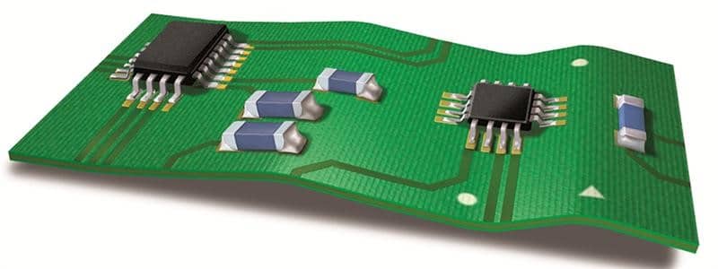
For proper placement of SMT components, it is necessary that the PCB remain perfectly flat. For accurate placement, the pick-and-place machine must release the SMT component at the same height above the board for all components. If the board has warpage, that is, it is not flat, the machine is unable to maintain a constant height when releasing the components while placing them on the board—this affects the accuracy of placement, especially for fine pitch components.
Additionally, a flat PCB helps retain SMT components in proper position during reflow. If the high temperature inside the reflow oven causes a change in the flatness of the board, the SMT component may slide out of position as they are afloat on molten solder, causing solder bridging and open circuits.
Read About: STOP THE DROP: FIXTURING A HEAVY SMT COMPONENT SAVES TIME, MONEY
The above situations result in low yields and higher rework for some boards during assembly. IPC has a High Temperature PCB Flatness Guideline, IPC-9841, a standard that provides local area PCB warpage information across reflow profile temperatures. The guidelines help in selecting necessary measurement equipment, planning testing, and preparing PCBs for test, and conducting measurements across reflow temperatures.
Controlling the flatness of a board is important for preventing issues related to assembly, including bridged or open joints, which ultimately cause product failure.
Causes of Warpage
PCB manufacturers are progressively using PCB substrates suitable for SMT, with good thermal stability, resistance to ion migration, low dielectric constant, good processing performance, and no substrate wandering, but high-end and offering green environmental protection. The current circuit board manufacturing technology ensures that warpage in a PCB remains within 0.5% in all states in the PCB assembly process.
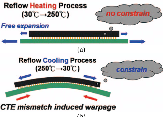
Stress causes warpage, one of the common problems in the PCB assembly process. During the production process, PCB substrates undergo expansion and contraction. However, the difference between expansion coefficients of the copper foil and the substrates is significant. This causes unequal expansion and contraction between the two, resulting in the generation of internal stresses. The release of these internal stresses causes warpage of substrates in the PCB.
Other factors that influence the extent of warpage in a multi-layered PCB are:
- Balance between the circuit area and the conductor pattern
- Symmetry of the circuit board stacking
- Weft direction of the inner layer and the cured sheet
- Operating temperature
Operating temperature has the greatest impact on warpage. During the PCB fabrication process, PCB products undergo several thermal excursions and heat treatments. As the processing temperature exceeds the Tg of the copper clad laminate, the fabricator must heat both sides of the substrate equally and uniformly, while keeping the processing time as short as possible to reduce warpage of the substrate.
Read About: DIFFERENT STACKUPS FOR HDI PCBS
The manner of storage and transportation of assembled PCBs also affects their warpage. Improper storage and transportation can cause other quality issues in assembled PCBs such as PCB surface discoloration and copper foil oxidation apart from plate bending. Store PCB assemblies preferably to prevent exposure to high temperatures, rain, and machinery damage, in a clean, dry, waterproof, fireproof, and on a non-corrosive flat surface.
Preventing Warpage
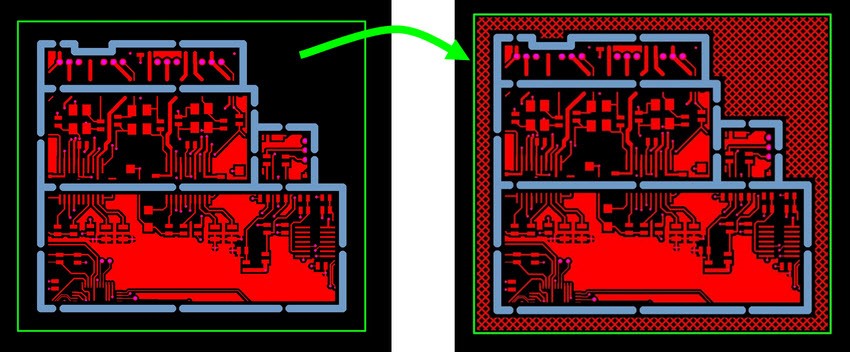
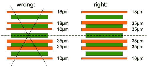
During fabrication of a PCB, there is even distribution among all dielectric layers. However, it is the uneven distribution of copper layers that causes PCB warpage to occur. To prevent warpage, the designer must balance the copper pattern on each layer of the board with the circuit area. The designer must also equalize the component layout, the assembly distribution, and the thermal distribution to decrease warpage.
For instance, if the outermost top side has a large copper surface while the outermost bottom side has only a few copper traces, the PCB will have a greater tendency to warp after etching. The designer must make sure the area of the line pattern on both the outer layers match as much as possible. If the copper areas on both sides differ by a significant amount, it is preferable the designer adds a separate copper grid on the thin side for balancing the two.
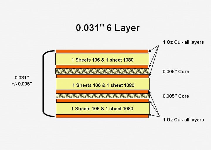
The fabricator must make sure to keep the arrangement of the interlayer prepreg symmetrical. For instance, for a six-layer board, the thickness between layers 1 to 2 and 5 to 6 should preferably be the same, including the number of prepreg sheets. This will prevent warping after lamination.
It is preferable the fabricator uses the same supplier for the prepregs and the multi-layer core sheets—this ensures the coefficient of expansion will be similar. After lamination, the warp and weft shrinkage rates of the prepreg may differ. Therefore, the fabricator must know the warp and weft directions before cutting and laminating. He/she must understand and make use of the latitude and longitude of the prepreg when using it for a multi-layered board to prevent warpage.
Usually, manufacturers wind the rolled prepreg in the warp direction, while keeping the weft direction across the width. For the copper foil sheet, however, they keep the weft direction along the long side, and the warp direction across the width. In case of doubt, the fabricator must clarify the above points from the manufacturer.
It is necessary for the fabricator to remove stress from the board after lamination. Typically, after hot and cold pressing, shearing and milling, the fabricator usually bakes a multi-layer board in an oven at 150 °C for four hours to release the stress in the sheets while the resin is in the process of curing. This is an important step to prevent warpage, and the fabricator must not miss this step.
The fabricator also must take precautions while plating. Both pattern and surface plating require the use of special nip rolls. As the multi-layered board may be ultra-thin, such as 0.4 to 0.6 mm thick, plating it requires clamping the board with a round stick to the flying plate of the automatic plating line—the clamping must extend to the entire flying bar. Usually, the operator will string the rollers together to keep the plates on the roll straight. Not doing this, and plating a copper layer of twenty to thirty microns on the sheet will make it bend, which is very difficult to remedy.
Conclusion
A non-flat PCB causes misalignment in the automated instrumentation line, as the SMT component will not land on the intended pads, components will not enter the intended hole in the board, and the warpage may even damage the automatic inserter machine. A bent circuit board is difficult to install in a chassis or a socket may misalign inside a machine, which makes it very troublesome for the assembler in a factory. This makes it very important for all stakeholders to take care to not allow warpage in the PCB.


