


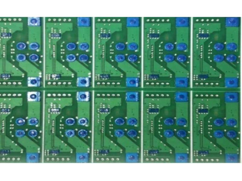
Peelable solder mask is a temporary protective coating used during printed circuit board (PCB) manufacturing and assembly to protect selected areas of the PCB from solder, flux, chemicals, and other processing materials. At Rush PCB Inc, we understand that peelable solder mask is specifically designed to be removed after the required manufacturing or assembly operation has been completed. This temporary protection makes it particularly useful for PCB areas that must remain free from solder during wave soldering, selective soldering, solder dipping, hot-air leveling, or other thermal processes. Peelable solder mask is also commonly referred to as peelable mask, temporary solder mask, or peelable coating
Composition and Material Characteristics
Peelable solder mask materials are generally formulated as polymer-based coatings designed to provide temporary mechanical and thermal protection. The exact formulation varies between manufacturers and applications, but the material typically contains a polymer resin system along with additives that provide flexibility, adhesion, thermal stability, and controlled peelability.
A major requirement of the material is that it must adhere sufficiently to the PCB surface during processing. If the coating separates prematurely, molten solder or flux may reach the protected area and cause contamination or solder deposition. At the same time, the adhesion must not be so strong that removing the mask damages the solder mask, copper surface, component pads, or other PCB features.
Thermal resistance is another important property. During wave or selective soldering, the PCB can be exposed to elevated temperatures for a relatively short period. The peelable mask must remain stable during this exposure without excessive melting, blistering, cracking, decomposition, or loss of adhesion. The material should maintain its protective function throughout the required process window.
Flexibility is equally important because the coating must be removed after processing. A suitable peelable mask forms a continuous film that can be lifted and removed without leaving excessive residue. Material selection therefore requires a balance between adhesion, flexibility, thermal resistance, chemical resistance, and clean removability.
Application of Peelable Solder Mask
The application process begins with preparation of the PCB surface. The board must be sufficiently clean and free from oil, dust, fingerprints, flux residues, and other contaminants that could interfere with adhesion. Surface preparation is important because poor adhesion may result in mask lifting or penetration of solder beneath the coating.
The peelable material can be applied using different methods depending on the production requirements, material characteristics, and equipment available. Manual application may be used for prototypes, repair work, or low-volume production, while automated dispensing or printing systems are more suitable for larger production volumes. The application equipment must provide accurate control of coating location, thickness, and coverage.
The mask is normally applied only to predetermined regions that require protection. The surrounding areas remain exposed so that soldering can take place normally. The coating thickness must be sufficient to provide complete protection without creating unnecessary material buildup around the edges of pads, holes, or other features.
After application, the material may require curing or drying depending on the specific formulation. Curing conditions such as temperature and time must be controlled according to the manufacturer’s requirements. Inadequate curing may result in poor mechanical strength, incomplete film formation, or premature removal during soldering. Excessive curing, on the other hand, may make the material difficult to peel and can increase the possibility of residue remaining on the PCB.
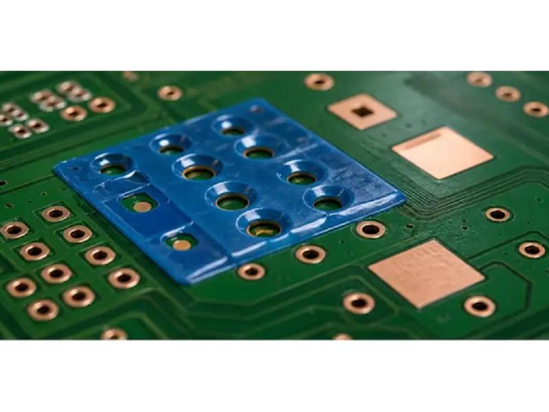
Peelable Solder Mask During Wave Soldering
One of the most common applications of peelable solder mask is protection during wave soldering. In wave soldering, the underside of the PCB passes through a wave of molten solder. The process is highly effective for soldering through-hole components but can expose many PCB surfaces to molten solder.
Certain areas must remain free of solder during this operation. Examples include gold-plated edge contacts, connector interfaces, selected test points, mounting areas, and specific through-holes that must remain open. Peelable solder mask can be applied to these areas before the board enters the soldering machine.
During soldering, the temporary mask acts as a physical barrier between the protected surface and the molten solder. The mask must remain intact throughout the soldering operation and must resist the combined effects of heat, flux, and mechanical forces generated by the process.
After soldering, the PCB is allowed to cool before the peelable mask is removed. The operator or automated process carefully lifts the coating from the protected region. Properly selected and applied material should separate as a continuous film, leaving the underlying surface clean and suitable for subsequent processing.
Peelable Solder Mask in Selective Soldering
Selective soldering is another important application of peelable solder mask. Unlike wave soldering, selective soldering uses a controlled solder nozzle to apply molten solder to specific through-hole locations. Although the process provides greater control, certain PCB regions may still require temporary protection.
Peelable solder mask can be used to protect nearby pads, connector areas, thermal-sensitive regions, or surfaces that must remain free from solder. The coating helps prevent accidental solder contact during the selective soldering process.
Because selective soldering may involve localized high-temperature exposure, the thermal resistance of the peelable material becomes particularly important. The coating must remain attached and intact throughout the soldering operation while still allowing clean removal afterward.
Proper mask placement is also important because excessive masking can interfere with solder flow or prevent the soldering nozzle from reaching the intended solder joints. Therefore, the mask pattern should be carefully defined according to the PCB assembly design and selective soldering process.
Peelable Mask Application Methods
Different application methods can be used depending on PCB geometry and production volume. Manual dispensing is a simple method in which the material is applied directly to selected regions using a controlled dispenser or suitable applicator. This method provides flexibility and is useful for prototypes, engineering samples, and small production quantities.
Screen printing can be used when the same masking pattern must be reproduced on a large number of PCBs. A stencil or screen transfers the peelable material onto predetermined areas. This method provides improved repeatability and can significantly increase production efficiency.
Automated dispensing systems are particularly useful for complex PCB designs where accurate material placement is required. Computer-controlled dispensing equipment can follow programmed coordinates and apply consistent quantities of material to selected areas. Such systems reduce operator variation and improve repeatability.
Regardless of the application method, the coating must be applied uniformly and must completely cover the intended protected region. Gaps, thin spots, bubbles, or incomplete coverage can allow solder or flux to reach the underlying surface and compromise the purpose of the mask.
Curing and Drying
Curing or drying is an important stage after application of peelable solder mask. The exact curing method depends on the material formulation. Some materials may dry at room temperature, while others require controlled heating or ultraviolet exposure.
During curing, the coating develops the mechanical and thermal properties required for the soldering operation. The process must be carefully controlled because insufficient curing can leave the material soft or weak, causing it to peel prematurely. Over-curing can produce excessive hardness or adhesion, making post-process removal more difficult.
Manufacturers must therefore establish a controlled curing process based on material specifications and production requirements. Temperature, curing time, humidity, and environmental conditions may need to be monitored to maintain consistent results.
A properly cured peelable mask should remain firmly attached during PCB processing but should still be removable without excessive force. Consistent curing is therefore essential for achieving reliable masking performance.
Removal of Peelable Solder Mask
Removal is one of the most important characteristics of a peelable solder mask. After completion of the required soldering or processing operation, the temporary coating must be removed to expose the protected PCB areas.
Removal is generally performed after the board has cooled sufficiently. The operator identifies an edge of the coating and carefully lifts it using an appropriate tool or by hand, depending on the material and manufacturing procedure. The coating should preferably come away as a continuous film rather than breaking into small fragments.
Clean removal is important because residual material can interfere with electrical contacts, soldering operations, connectors, or subsequent coating processes. Manufacturers may therefore inspect the PCB after removal to ensure that no significant residue remains.
The ease of removal depends on material selection, surface condition, coating thickness, curing conditions, and processing temperature. If the coating has excessive adhesion or has been incorrectly cured, removal may become difficult and could potentially damage delicate PCB features.
Common Defects in Peelable Solder Mask
Several defects can occur during application and processing of peelable solder mask. One common defect is incomplete coverage, where a portion of the intended protected area remains exposed. This may allow solder to reach the PCB surface during wave or selective soldering.
Another defect is poor adhesion, which may cause the coating to lift or peel during soldering. Poor adhesion can result from surface contamination, inadequate surface preparation, incorrect curing, or incompatible materials. If the coating separates during processing, solder or flux may penetrate underneath it.
Bubbles and pinholes are additional concerns. Air trapped inside the coating can create weak points and may expose the underlying PCB during thermal processing. Excessive coating thickness can also cause uneven curing and make removal more difficult.
Residue after peeling is another potential problem. Residual material may remain on pads or contacts and interfere with electrical or mechanical functions. Manufacturers should therefore inspect masked areas after removal to confirm that the surface is sufficiently clean.
Advantages of Peelable Solder Mask
Peelable solder mask provides several advantages in PCB manufacturing. The most important advantage is its ability to protect selected areas without permanently covering them. This provides manufacturers with greater flexibility when different regions of the same PCB require different processing conditions.
The material can also reduce the need for manual masking methods such as adhesive tapes, plugs, and mechanical shields. Compared with these methods, a properly applied peelable coating can provide more precise coverage and better adaptation to complex PCB geometries.
Another advantage is improved process efficiency. Once the material has been applied and cured, the PCB can proceed through the required soldering process without requiring additional manual protection during the soldering operation. The mask can then be removed afterward.
Peelable solder mask is also useful for rework and repair operations. Selected areas can be temporarily protected while another portion of the PCB undergoes soldering or thermal processing. This makes the material valuable not only in mass production but also in prototype development and repair environments.
Limitations of Peelable Solder Mask
Despite its advantages, peelable solder mask has several limitations. The application process introduces an additional manufacturing operation that requires material handling, application equipment, curing, inspection, and removal. These activities can increase production time and labor requirements.
The material must also be carefully selected for the intended soldering process. A peelable mask that does not have adequate thermal resistance may soften, blister, crack, or lose adhesion during soldering. Similarly, a material with excessive adhesion may be difficult to remove after processing.
Another limitation is the possibility of residue. If the material is incorrectly applied or cured, remnants may remain on the PCB after peeling. Such residue can interfere with connectors, test points, soldering, or electrical contacts.
The coating can also become damaged during handling before soldering. Scratches, cuts, or partial lifting may reduce its protective effectiveness. Therefore, proper handling and inspection are necessary throughout the manufacturing process.
Conclusion
Peelable solder mask is an important temporary protection technology used in PCB manufacturing and assembly. Unlike permanent solder mask, it is specifically designed to protect selected PCB areas during processes such as wave soldering, selective soldering, and other thermal or chemical operations and can subsequently be removed to expose the underlying surface.
The effectiveness of peelable solder mask depends on proper material selection, surface preparation, application, curing, thermal resistance, and removal characteristics. A properly controlled process prevents unwanted solder deposition and contamination while allowing protected areas to remain functional after assembly.
Although the process introduces additional material and handling requirements, its ability to provide selective temporary protection makes it a valuable solution for complex PCB assemblies. Trust the specialized expertise at Rush PCB Inc for your PCB manufacturing needs. With continued advances in materials, automated dispensing, machine vision, and digital manufacturing, peelable solder mask technology is expected to remain an important part of modern PCB manufacturing and assembly processes.


