

PCBs – Interesting Facts
PCBs are older than you’d think: The concept of a PCB is 80 years old! The first PCB was designed by an Austrian (Paul Eisler) inventor in 1936. He used the board in a radio set. The boards only became common from the 1950s, when mass production of electronics such as radios and television sets changed the world.
They’re a part of our lives, everywhere, everyday: We’re always aware of PCBs being present in computers. But they are in almost every device we now use. For most people, there is be a PCB within reach at most times of the day – in your phone, your car… everywhere.
There are basic designs: Almost all PCBs can be specified within the parameters of 14 standard services. The use of standard specifications reduces manufacturing costs.
Read About:ESSENTIAL FACTORS AFFECTING THE COST OF PRINTED CIRCUIT BOARDS MANUFACTURED BY RUSH PCB INC.
They are fully customizable: Circuit boards can be made to meet anyone’s specific requirements (although this is an expensive option).
There are many different components: batteries, LEDs, diodes, inductors, resistors, transistors, transformers, relays, capacitators, potentiometers, fuses and switches.
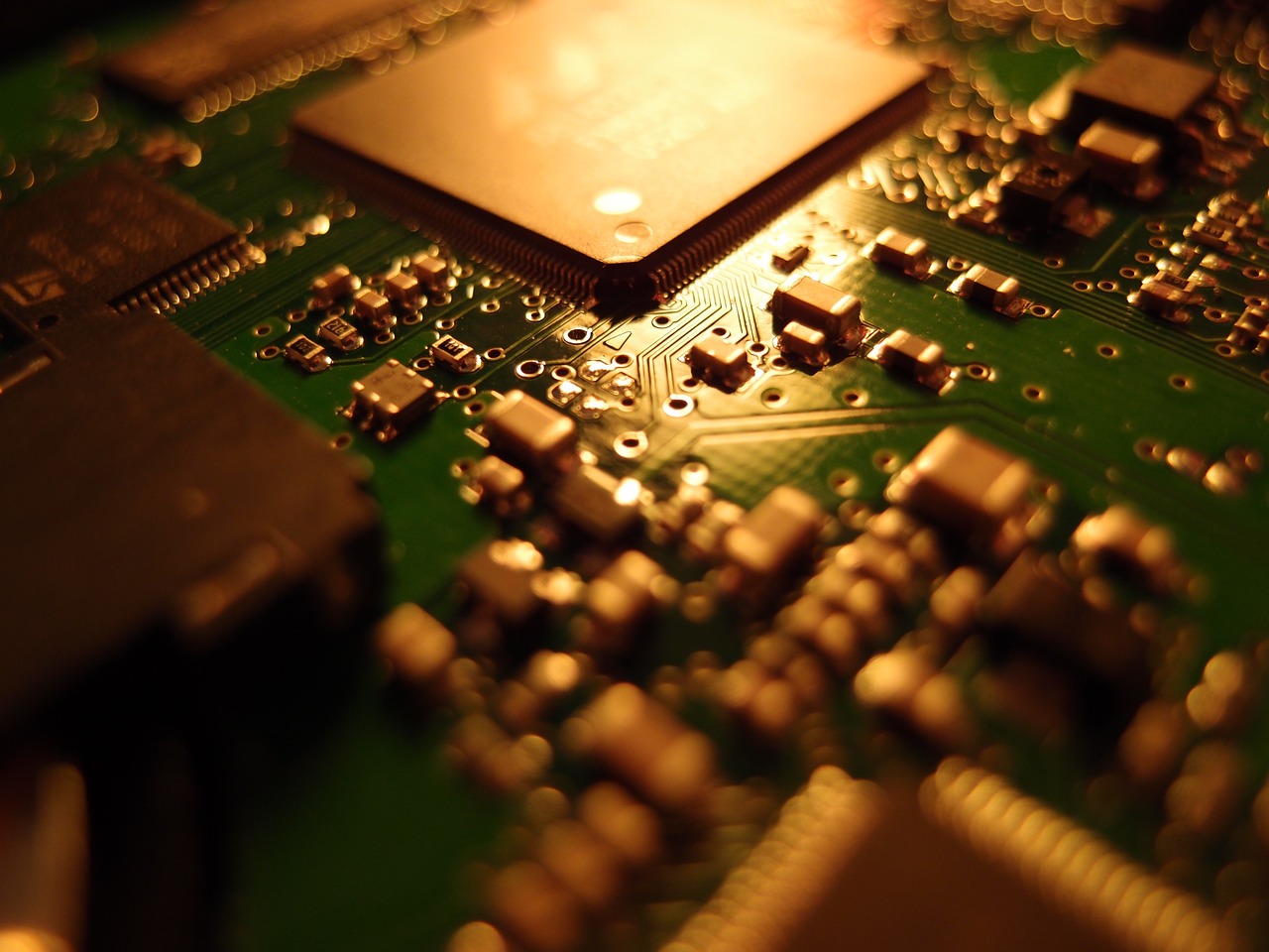
They are green! Original PCBs were green due to the solder mask resins. While the technology has changed, the color hasn’t. It has been suggested that green is a good color, as it allows electrical engineers to easily see faults in the traces.
They don’t use wires: Wires take up too much space. In their place, PCBs use copper ‘traces’. This allows PCBs to be much smaller.
Change is Constant: Circuit boards have clearly changed since Paul Eisler first designed one. The technology over the years has been a steady reduction in size, corresponding to an increase in speed. Surface Mount Technology (SMT) has allowed for a reduction in size by an order of magnitude over through-hole mounting.
Graphene technology is likely to make considerable change: Graphene is a two-dimensional array of atomic-scale carbon atoms. The use of graphene is likely to considerably reduce the size and increase the performance of future PCBs.
They can be built in layers: Original PCBs had all circuits on one side. As SMT doesn’t affect both sides of the board, both sides can be used to host components. In addition to double-sided PCBs, layers can be laid on top of each other on the same side, increasing capacity.
Another layer is the silkscreen: These are the white etchings Not etched screen printed (readable text) that sit on top of the solder mask. The silkscreen has letters and numbers drawn onto it to allow for more simple assembly. Historically, the text was printed with a silk screen printing process. Today, it is more likely that the printing is done by ink-jet printers.
They are made twice: The first time a PCB is made, it is developed in a Computer Aided Design (CAD) program. The software will test the layout to ensure that the connections all work and perform as intended. Once the engineer is sure that the PCB is operating correctly, the physical board is made.
New technology means that PCBs may in future be biodegradable!


