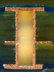
In the first half of this column, we began a discussion of the pros and cons regarding the use of conductive inks versus nonconductive inks to fill vias. The images below show cross-sections of a via-in-pad with nonconductive ink on the left and VIP with conductive ink on the right.
In that column, we discussed a design that required a nonconductive ink in the through-hole via and conductive ink in the blind via. Now we ask, what were the drivers behind this decision? Why would one use two different types of inks in vias in the same PCB, and why conductive vs. nonconductive ink? The answers are actually a bit more complex.
Copper plating is one factor, as an example. For years it has been generally accepted that copper plating is not a viable substitute for ink (conductive or nonconductive) to fill a through-hole via, buried via, or blind via. It was believed that to plate a via shut and to cover the surface with copper would take “forever,” relatively speaking, if it could be done at all.
One reasoned that not only would the process of plating the via shut with copper be prohibitively time-consuming, but even if it were technically possible to fill the hole with plated copper, the unwanted consequence of plating so much copper in the hole would result in excessive “button” or surface copper height that would lead to other defects and/or reliability risks.
Nowadays there are several efficient processes for copper plating to fill vias; two of these are pulse and DC rectification. Some require button plating, a two-stage process; others have evolved to the point where a single-stage panel plate will fill certain via structures while depositing less material on the surface, thereby leaving a manageable surface copper thickness. In this way, one can continue to produce a high-density product without the need for a secondary ink-filling operation.
Read About:IPC STANDARDS FOR PCBS
Further, there are solutions to filling micro, blind and buried vias that require no additional process time or steps; e.g., resin or B-stage fill. The consensus was that it wasn’t possible to do this reliably. While conventional prepreg (B-Stage) historically struggled to fully and consistently fill vias, there are now specialized prepregs and bonding materials specifically engineered to do just this process reliably.
One laminate company produces a series of FR-4, lead-free, polyimide, low-loss and other high-performance laminates and prepregs. Within their product line they offer a sub-set of prepreg (B-Stage) called the VF-series (whereby VF is an abbreviation for via fill).

Via Fill (VF) prepreg product, where core and prepreg are combined to create a pure, homogeneous material package.
Where we have the instance of a buried via filled with one ply of VF material, the blind via is fully filled with resin, and the dielectric distance between outer foil and inner sub assembly is very uniform. In this case, the VF matches the family of core and prepreg it is combined with, so that it permits the creation of a pure homogeneous material package, eliminating the need for a hybrid material / laminate package. The VF prepreg has been engineered for enhanced rheology and filler content so that during the lamination process the blind and buried vias found in a sequential lamination sub assembly will be fully filled.
VF Prepreg is just one example of available materials designed to fill vias during the lamination process, thus eliminating the need for a secondary operation. What process and material should you use? To make the best decision, you need to understand not just what result you want to achieve, but why.
Not long ago I had an application involving a customer’s requirement of a specific brand of conductive ink to fill a small through-hole via. The assembly was a double-sided PCB on a relatively thin (0.010″ thick) PTFE/Teflon material.
The ink-filling process requires a planarization or sanding operation after the ink is cured in order to remove excess ink from the copper surface. The planarization process always includes some inherent risks and/or limitations such as:
- Dimensional distortion of the panel of PCB material.
- Imprecision, resulting in uneven copper thickness and poor control of circuit etching.
- Reduced peel strength of the surface copper.
In this case, all these negative aspects of planarization were amplified because the material was a soft; thin Teflon with RA copper. This material is highly unstable to begin with and susceptible to distortion.
The PCB manufacturer struggled to meet the customer’s requirements, but excess cost, time to produce, delays, and lower yields resulting when compliant product was finally produced were a real problem, prompting further discussion with the customer.
A breakthrough occurred when we began to ask why we were using certain materials and questioned the necessity and benefit of each step in the process. We realized that the via filling; i.e., the specific material requested by the customer, was being used to prevent solder from flowing through the vias during assembly. But what else was it there for?
After critical examination, we realized:
- That there was no need for conductivity in the filling material , let alone any reason for it to be limited to the customer’s specifically preferred ink material.
- There was no need for a copper pad to be plated over the surface of the material or via, since nothing was being soldered on top of the via.
- There was no need for a specific brand of ink material.
- Alternative materials and processes could therefore be explored.
After all, we began to examine the real purpose that the via filling was intended to address, and more importantly, what it was not there for. The material had been used, all along based upon a group of assumptions that, when examined, weren’t true and did not justify the use of that specific (and costly) ink material. Its use simply could not stand up to challenging questions, such as added reliability, electrical advantages or mechanical aspects or even thermal characteristics or properties. It contributed to none of these justifying criteria.
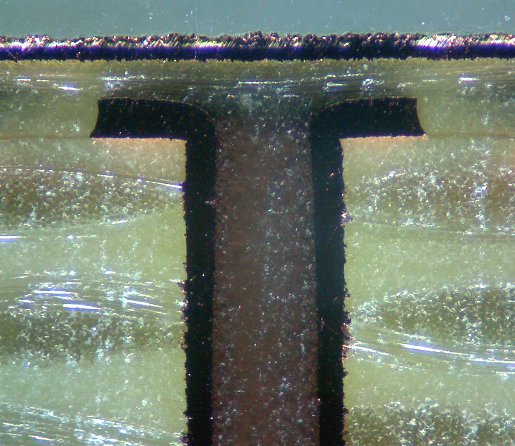
Buried via fully filled with resin; note that the dielectric thickness between the outer foil and the inner subassembly is very uniform.
In summary, when evaluating a new product, manufacturing process, etc.:
- Challenge any long-held assumptions.
- Gather information from multiple sources.
- Qualify that what you have been told by others is really best for your needs and not skewed merely to support the choice of a specific product.
Manufacturers must talk with the designer to understand what designers really want to accomplish and why. Designers must speak with manufacturers in order to understand the intricacies of the process. Finally, as technology evolves and more innovative solutions for emerging applications or enhanced solutions for existing ones are found, cooperation and collaboration are the keys to optimizing decisions and selections.


