

Most IC packages have soldering pins along one, two, or all four of their edges. While some have them positioned away from the body, for some the manufacturers bend the pins back under the package body. These packages have names such as SOP, TSOP, QFP, TQFP, and more. With rising demand for increasing functionality from ICs, manufacturers have introduced a new type of package that has solder balls on its underside rather than pins for soldering. The name of this package is BGA or Ball Grid Array.
As the name suggests, rather than using pins, the BGA is a surface mount chip package with balls of solder arranged in an array on its underside. While reflow soldering, the balls melt to form electrical connections between the device and pads, also arranged in arrays, on the PCB. The advantage in using balls of solder arranged in a grid form is the underside of the package can carry a much higher count of balls compared to the number of pins on all the four sides together.
Compared to the perimeter style mounting, BGA packages therefore offer a much smaller footprint on the PCB, apart from providing better electrical and thermal properties. According to Rush PCB, the resulting miniaturization has increased the popularity of BGA in the electronic industry.
Integrated circuits working at high frequencies benefit from the low lead inductance and the unparalleled pin density of the BGA packaging. However, the pin density of the BGA comes as a challenge to PCB designers, since they must find innovative means of breaking out the electrical connections from under the device.
The Challenge of the BGAs
Earlier, BGAs had larger pitch and spacing between their solder balls. Bringing out traces from the BGA pins to connect to other components on the board did not pose a problem, as designers could easily route numerous traces between two neighboring pins.
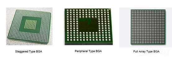
BGA packages also have variations. While some of them do not have pins in the center, others have them all over the bottom of the package. With the pin count going up, the pitch and spacing has been steadily decreasing and designers are finding it more and more difficult to route traces between the pins.
Designers have tried to get around this problem by increasing the number of layers, but this has the undesired effect of increasing the cost of the board. Therefore, designers must be more innovative in their approach and increase the layer count only as a last option. Moreover, the optimal fanout depends on the ball pattern on the device and the board.
The ball pattern is not identical for all BGA ICs. While some may have them parallel and equidistant, for others the spacing may be greater in one direction than in other. The designer must consider the spacing between the balls for the specific BGA IC and the minimum trace width and spacing that they must maintain.
Vias to the Rescue
One of the methods designers deploy to route connections from BGA pads is to use vias. However, the use of vias must be judicial and the designer must know where and how to place them. For instance, using through vias drilled with mechanical drill bits may cut down on expenses, but reduce the reliability of the board. The best option for the designer is to use blind vias drilled with lasers. The industry calls them microvias, and the advantage is the designer has the option of drilling down to the layer necessary for the connection. It is also possible to laminate the buried via to enable it to change layers within the PCB. Although the microvia technology is expensive, eminent PCB manufacturers such as Rush PCB have mastered it through long experience.
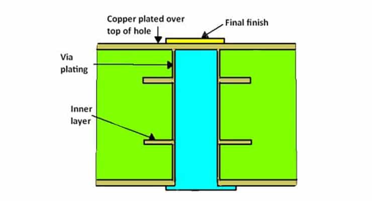
The designer must be aware that placing a via in the pad of the BGA in a PCB is a recipe for disaster. If the via does not have solder mask covering it, it will wick molten solder away from the pad during reflow, causing the BGA to fail due to poor solder joints. Therefore, if the designer places via on the pads, they must also take care to cover them with solder mask, or fill the via hole and plate the top to close it.
BGA Placement and Soldering
Most pick-and-place machines are capable of handling BGA and QBGA packages for machine assembly in much the same manner as they handle other surface mount components.
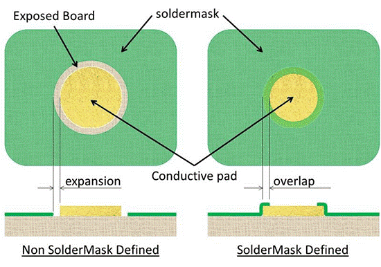
Designers use different types of pads on PCBs for connecting to BGAs—pads defined by solder mask and pads defined by copper. For pads defined by solder mask, the solder mask encroaches on the pad, whereas it does not do so for the other. Rush PCB recommends designers use pads defined by copper (also known as non-solder mask defined pads) as they offer increased surface are for soldering. However, when using BGAs with finer pitches, the designer should use solder mask defined pads, as they decrease the chances of solder bridging.
As the solder balls are present on the underside of the BGA and connect to the PCB immediately underneath, it is not possible to manually solder the BGA IC. The only options available to the assembler is to use infrared heating or a reflow oven. Compared to the localized heating of the soldering iron, the reflow oven or infrared heating causes a more even distribution of heat, melting all the solder balls simultaneously. This method allows automatic alignment of the IC as the package virtually floats on the molten solder balls and aligns itself with the pads on the PCB, while the solder solidifies. As the body of the package on one side, and the PCB on the other sandwich the solder balls, they are not visible after soldering, and hence, it is not possible to visually inspect them.
Read About: WHAT IS A SOLDER JOINT?
Inspecting and Testing BGAs
Unless testing stations use specialized equipment, it is impossible for them to find a solder fault beneath a BGA device after the assembly process has soldered it into place on a PCB. The specialized equipment necessary are JTAGs, endoscopes, special microscopes, industrial CT scanning machines, and X-ray machines.
The most useful inspection equipment among the above is the X-ray machine with 2D and 3D vision capability. With an X-ray machine, it is possible to inspect for missing solder balls, solder bridging, misalignment, solder wicking, excess solder, and the presence of solder balls. However, the X-ray inspection method can only verify if the assembly process has placed each solder ball properly, that each solder ball has made contact with the pad, and there has been no solder wicking. Once the X-ray process certifies correct soldering of the BGA, the testing process can begin.
Conclusion
Overall, it may seem using BGAs is a difficult process. However, the increased performance of the device and the amount of space it saves easily overcomes the complexity and difficulty in using BGAs. At Rush PCB, we offer our experience and technical knowledge in BGA and QBGA handling and assembly to our customers. Please contact Rush PCB today for all your requirements of PCB design and assembly with BGA and QBGA.


