


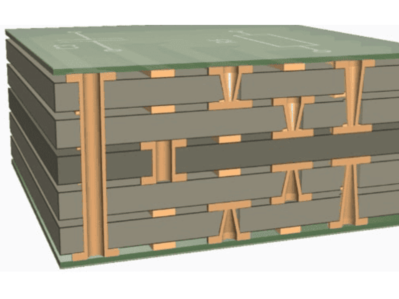
In the world of PCB design, annular rings play a critical role in ensuring reliable connections and structural integrity, especially in through-hole via design. An annular ring is the copper area surrounding a drilled hole or via on a printed circuit board (PCB), providing a strong electrical and mechanical connection between layers and components.
What Is an Annular Ring?
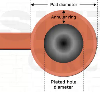
An annular ring is the circular copper pad that surrounds a drilled hole or via on a PCB. At RUSH PCB Inc, we consider it a key structural element as it acts as a landing area for connecting traces or components to the via, ensuring a solid electrical and mechanical bond. In through-hole via design, the annular ring is especially crucial because it supports the soldering process, where component leads are inserted through the hole and soldered to the pad.
The size and shape of the annular ring directly impact the reliability of the connection. A well-designed annular ring provides enough copper area for soldering or plating, while a poorly designed one can lead to issues like weak connections or manufacturing defects. For instance, if the annular ring is too small, it might not provide sufficient space for solder to adhere properly, leading to potential failures in the circuit.
Annular Ring = (Pad Diameter − Finished Hole Diameter) / 2
Importance of Annular Ring
The annular ring provides several important functions in PCB construction. First, it provides sufficient copper area for establishing a reliable electrical connection between the plated hole and the circuit layer. Second, it contributes to the mechanical strength of the connection. Third, it provides manufacturing tolerance for positional variations during imaging, lamination, drilling, and other fabrication processes.
An adequate annular ring is particularly important for multilayer PCBs because a plated through-hole may need to connect to copper pads on several internal layers. If the hole is slightly displaced, the available copper around one or more internal pads may become smaller. If the displacement is excessive, the hole may partially or completely break out of the pad. Thus, annular ring and PCB registration are closely related manufacturing parameters.
Types of Annular Ring
Internal Annular Rings
These are found on the inner layers of a multi-layer PCB. They are critical for connecting different layers through vias. The internal annular rings must be precisely aligned and manufactured to ensure reliable inter-layer connections.
External Annular Rings
These are located on the outer layers of the PCB and are typically visible. They are used for mounting components and connecting the components’ leads to the PCB traces. These rings must withstand soldering processes and provide robust mechanical and electrical connections.
Microvia Annular Rings
Microvias are used in high-density interconnect (HDI) PCBs. They are smaller than traditional vias and typically laser-drilled. The annular rings around microvias need to be very precise to maintain connectivity in the densely packed PCB layout.
Factors Affecting Annular Ring
Drilling accuracy is one of the most direct factors. CNC drilling machines must position holes accurately according to the manufacturing data. Machine calibration, spindle runout, tool condition, vibration, panel fixation, and drilling parameters can influence hole position.
PCB material movement is another major factor. Laminates can expand or contract due to temperature and moisture. During multilayer fabrication, the panels are exposed to heating and pressure during lamination, followed by cooling. These conditions can change the dimensions of the panel and alter the relative position between internal copper features and drilled holes.
Artwork and imaging accuracy also influence annular ring. If the copper pad is not formed at the correct position during imaging or etching, the final pad dimensions and location may differ from the intended design. Etching can further reduce copper dimensions, especially when fine features are involved.
Effect of Lamination on Annular Ring
Multilayer PCB lamination can significantly influence registration and annular-ring performance. During lamination, prepreg resin flows under controlled temperature and pressure to bond the individual layers together. The different materials used in the PCB construction have different thermal and dimensional characteristics.
Copper distribution also affects panel movement. A panel with an uneven distribution of copper may experience different dimensional behavior compared with a balanced panel. Manufacturers therefore consider copper distribution, laminate construction, press parameters, and material characteristics when developing compensation factors for multilayer manufacturing.
If the internal layers move during lamination and the subsequent drilling operation does not compensate for this movement, the holes may become displaced relative to the internal pads. This can result in reduced annular rings or hole breakout.
Annular Ring in Multilayer PCBs
Multilayer PCBs require more careful annular-ring control than simple single- or double-sided boards. A through-hole may connect multiple internal copper layers, and each layer may have slightly different registration relative to the drilled hole. Consequently, a hole that appears well centered on the outer surface may have a reduced annular ring on one or more internal layers.
As the layer count increases, the number of manufacturing variables also increases. Inner-layer imaging, etching, lamination, drilling, and material movement must all be controlled. Accurate tooling, dimensional compensation, and registration inspection are therefore essential for maintaining consistent annular rings across the entire board.
Annular Ring in HDI and Microvia PCBs
Modern HDI PCBs present additional challenges because microvias and their associated pads are significantly smaller than conventional through-hole structures. A small positional error can consume a large percentage of the available annular-ring margin.
In microvia structures, the laser-drilled via must accurately land on the underlying copper pad. If the microvia is displaced too far, insufficient copper may remain around the connection. This can reduce the reliability of the interconnection and may result in an open connection or other structural defect.
Sequential buildup processes further increase the importance of registration control because each additional layer must be aligned with the previously manufactured structure.
Inspection of Annular Ring
Several inspection techniques can be used to verify annular-ring quality. Automated optical inspection (AOI) can inspect suitable external features and identify dimensional or positional problems. However, AOI has limitations when internal-layer structures are involved.
X-ray inspection can be used to examine internal-layer registration and determine whether drilled holes are correctly positioned relative to buried copper pads. This is especially useful for complex multilayer and HDI structures.
Microsection analysis provides a direct cross-sectional view of the hole and surrounding copper. The board is cut through the relevant feature, prepared through grinding and polishing, and examined under magnification. Microsection analysis can reveal the actual annular ring, copper plating thickness, hole-wall quality, internal-layer registration, and breakout conditions.
Common Annular Ring Defects
Even with careful planning, issues with annular rings can arise during PCB design or manufacturing. Here are some common problems and strategies to mitigate them:
Insufficient Annular Ring Width: This can lead to weak solder joints or poor plating. To avoid this, always design with a width above the minimum specified by your manufacturer, ideally 0.25 mm (10 mils) or more for standard designs.
Misalignment During Drilling: Misalignment can cause tangency or breakout. Work with manufacturers who use high-precision drilling equipment, and design with larger pads to provide a safety margin.
Thermal Damage: Excessive heat during soldering can damage the annular ring or surrounding traces. Use thermal relief patterns, such as spokes connecting the ring to large copper planes, to manage heat dissipation effectively.
These defects may result from a combination of factors rather than a single manufacturing problem. Therefore, root-cause analysis should consider design dimensions, registration, material movement, drilling, and plating processes together.
Prevention of Annular Ring Problems
The most effective method of preventing annular-ring problems is to establish sufficient design margin. Pad sizes should be selected based on the finished hole diameter and expected manufacturing tolerances. Manufacturing capabilities should be considered before committing to extremely small annular-ring designs.
Material selection and lamination control are also important. Stable laminate materials and consistent press conditions can reduce unpredictable dimensional movement. Copper balancing can further improve dimensional stability in multilayer panels.
Regular drilling-machine calibration, proper drill-tool maintenance, accurate tooling, and appropriate drilling parameters help maintain hole-position accuracy. Registration monitoring and microsection analysis can be used to verify that the manufacturing process is consistently meeting requirements.
Conclusion
Annular ring is a fundamental feature of PCB construction that directly influences the electrical and mechanical reliability of drilled and plated interconnections. It provides the copper area required around a finished hole and also serves as an important manufacturing tolerance against positional variation. Maintaining an adequate annular ring requires coordinated control of PCB design, imaging, lamination, drilling, tooling, material stability, dimensional compensation, and inspection.
As PCB technology continues to move toward smaller holes, finer features, HDI structures, and higher layer counts, annular-ring control becomes increasingly challenging. Accurate drill-to-pad registration, stable materials, controlled lamination, properly maintained drilling equipment, and effective inspection techniques are therefore essential. By incorporating sufficient design margins and maintaining tight manufacturing-process control, PCB manufacturers like RUSH PCB Inc can minimize annular-ring defects, reduce the risk of hole breakout, and improve the overall reliability and performance of printed circuit boards.


