

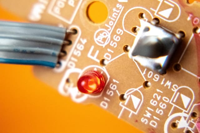
Printed Circuit Board or PCB manufacturers like Rush PCB Inc use various materials for cladding boards. One of the most common materials for cladding is copper. The main reason for this is copper is a good conductor of electricity and heat. A PCB serves two basic functions in a device. First, it provides an adequate support for mounting the electronic components that make up the circuit, and second, it also provides the electrical interconnections between the electronic components to allow them to function together.
What is a Copper Clad Laminate
A laminate with a thin sheet of copper bonded onto one or both its sides is a copper clad laminate. PCB manufacturers use this copper clad laminates as the core in making multilayer boards. The core provides the mechanical support for the entire board. The manufacturer may add more layers on either side of the core as necessary. These layers consist of prepreg and a copper layer bonded on the core.
In most cases, the laminate is usually a woven glass fiber sheet impregnated with epoxy resin. Manufacturers use copper clad laminates as the most common and significant substrate while fabricating PCBs. This is true whether the board is for industrial use or consumer electronics use. They also use other substrate materials. These include paper, fiber cloth, and paper pulp.
Types of Materials for Copper Clad Boards
Manufacturers use various types of materials for copper clad boards. Some of these materials are:
FR-4
This is one of the most common materials that manufacturers use as substrate for copper clad boards. It is cheaper than most other materials and has fairly good properties. The name is an acronym for fire retardant. It has good thermal conductivity, a high glass transition temperature, and a low coefficient of thermal expansion.
CEM
This is composite epoxy material, grade 3, and is typically used in place of FR-4. Mechanically, it offers a lower endurance as compared to FR4. However, CEM is lighter than FR4 and cheaper, which makes it a cost-effective alternative.
Copper Foil
This is usually electrolytic copper that manufacturers deposit on a thin layer on the base of the board. When bonded on to the insulating substrate, the arrangement becomes a copper clad board.
Prepreg
This is the additional layer for building up the additional layers of a multilayer board. It is typically fiberglass pre-impregnated with epoxy resin. Initially, the manufacturer does not totally cure the resin. Once placed on the core, with a copper foil on top, the fabricator applies pressure and heat to make the layers bond. The heat and pressure makes the resin flow, and the prepreg bonds with the copper foil of the layer below it and the copper layer above it.
Using a Copper Clad Laminate for a PCB
A designer typically transfers the circuit to the copper layer on a PCB. For this, they must arrange the circuit suitably, by using various PCB design software. The process has several steps:
Circuit Schematic
Initially, the designer starts with a circuit schematic. They use standard symbols for each electronic component from the software library to form the circuit schematic. Each component has a number of nodes representing its leads. A net list represents the interconnections between the leads of various components.
Board Layout
Depending on the physical space available for the board in the system, the designer makes a board outline. They download the footprint of all the components in the schematic from the library of the design software. After spacing them within the board outline, the designer now routes the various connections between the leads.
If space permits, the designer can accommodate all interconnections on one layer. Else, they design a multilayer board. They transfer some interconnections to inner layers, and use vias to interconnect them. The designer then transfers the board layout to Gerber files as output. They transfer the Gerber files to the PCB manufacturer.
PCB Manufacturing
The manufacturer uses the Gerber files to transfer the circuit to the copper clad. They may use direct transfer or photographic methods. The circuit represents the copper tracks that will interconnect the various components on the board. The manufacturer places a preventing coating on the circuit paths and subjects the copper clad to chemical etching.
The chemical etching process removes the unprotected extra copper, leaving the required circuit connections on the board. This transforms the copper clad into a printed circuit board.
Conclusion
Printed circuit boards offer mechanical support to electronic and mechanical components necessary for electronic devices to function. The board also provides the interconnections necessary for the electronic components. A copper clad laminate forms the basis for manufacturing a printed circuit board. Eminent PCB manufacturers like Rush PCB Inc use copper clad PCB boards for making various types of printed circuit boards.


