

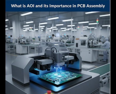
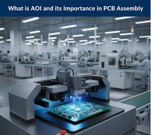
AOI, an acronym for Automated Optical Inspection, is a crucial process in the assembly of printed circuit boards or PCBs. Using high-resolution cameras, the non-contact inspection method utilizes advanced image processing software to detect and identify defects on PCBs. With AOI systems, we, at Rush PCB Inc., inspect PCBs at various stages of the assembly process, including post-placement and post-reflow.
Why AOI?
Automated Optical Inspection enables ensuring the quality and reliability of PCBs. It does so by identifying defects like missing components, improper component placements, inadvertent solder bridges, solder balls, and many other assembly flaws. Detecting such defects early in the assembly process means the manufacturer can reduce the cost of rework or scrap, thereby improving product quality, production throughput, and efficiency.
How AOI Works?
To use AOI systems effectively, the manufacturer must have the following components:
- A conveyor system
- Proper lighting
- High-resolution cameras
- Image processing software
The Automated Optical Inspection systems work in four steps:
1. Image acquisition
A conveyor system moving through the AOI machine carries the PCBs through it. While passing through, high-resolution cameras capture images of the board from various angles. Effective lighting on the board is necessary for the cameras to capture clear and sharp images.
2. Image Processing
The image processing software then analyses these captured images. It compares them to the inspection criteria that is available with it as a pre-defined set. The inspection criteria depend on the PCB CAD data, specifications, including parameters such as conductor spacing, solder joint quality, and component placement.
3. Finding Defects
The image processing software finds deviations by examining shapes, dimensions, and patterns. It contrasts them with the pre-defined set of data, detecting issues such as solder bridges, open circuits, missing components, and misplaced parts.
4. Reporting and Output
The software flags any deviations from the inspection criteria, sending an alert to the operator. The system provides a thorough summary of flaws along with visual clues to the defects, flagging them for operator assessment or automated sorting.
Types of AOI Systems
Typically, there are three main types of AOI systems in use in PCB assembly. These are:
2-D AOI
The 2-D AOI system uses only a single camera to capture images of a board. It does so from a top-down perspective. These systems are the least expensive types and are useful for inspecting component placement and solder joints. However, these systems are incapable of detecting defects in the z-axis, like tombstoning and lifted leads.
3-D AOI
This is a more advanced system and uses multiple cameras to capture several images of the board from various angles. This method helps to create a 3-D representative image of the board, capable of detecting a wider range of defects, including tombstoning, lifted leads, in addition to solder joint defects. Although more expensive than 2-D AOI systems, 3-D AOI systems offer higher reliability and greater accuracy.
Laser AOI
The latest Automated Optical Inspection systems use a laser to scan the board surface. This creates a high-resolution 3-D image of the board, capable of detecting even the smallest defects like hairline cracks. Being the most expensive type of AOI systems, laser AOI systems offer the highest levels of reliability and accuracy, capable of detecting even voids in solder joints.
Importance of AOI in PCB Assembly
During PCB assembly, the Automated Optical Inspection systems bridge the gap between precision and efficiency. They not only enhance the quality aspect but also drive up profitability. As such, these systems offer several critical advantages over conventional manual inspection processes:
- Enhanced Precision: By precisely detecting even the tiniest defects, AOI is superior to human inspection methods prone to errors.
- Higher Throughput: Reduced inspection time per PCB improves production efficiency.
- Cost-Effective: Early and thorough fault diagnosis further lowers expenses for rework and scrap, while reducing labor costs by improving productivity.
- Data Collection and Analysis: These systems typically generate large amounts of detailed inspection data, which is useful for process and quality improvement.
- Scalability: Automated Optical Inspection systems are useful for both small-batch and large-scale production.
- Non-Contact Process: There is no manual handling of the PCB, thereby guaranteeing no physical harm to it during inspection.
- Quick Feedback: Fast insights enhance production efficiency.
- Compliance with Industry Standards: AOI systems ensure compliance with industry standards such as IPC-A-610 and others.
How AOI Compares with Other Inspection Methods
Manufacturers use other inspection methods during the manufacturing and assembly of PCBs. Typically, these are:
- Manual Inspection
- Automated X-ray Inspection
- Functionality Testing
Among these, functionality testing confirms operational performance, while automated X-ray inspection is good for detecting internal defects. Therefore, AOI compares directly only with manual inspection methods for detecting surface defects and is superior in being quicker and more reliable. Moreover, AOI is less likely to contain errors brought on by human weariness.
Defects Detected by AOI During PCB Assembly
AOI is capable of detecting various types of defects related to different issues, such as:
Dimensional Errors:
-
- Inconsistencies in pad sizes
- Variations in trace width
- Conductor Spacing Violations
Surface Defects:
-
- Warping
- Contaminants
- Scratches
- Hairline Cracks
Component Issues
-
- Incorrect Polarity
- Misaligned Components
- Missing Components
- Tombstoning
- Lifted Leads
Soldering Issues
-
- Cold Solder Joints
- Extra Solder
- Solder Bridges
- Insufficient Solder
- No Solder
- Voids in Solder Joints
AOI Deployment in PCB Assembly
Certain stages benefit the most from AOI deployment. Detecting defects at these stages has the maximum effect due to early detection and process correction. Manufacturers typically deploy AOI systems at the following key stages:
- Pre-Placement Inspection
This is the stage immediately after solder-paste deposition and prior to commencement of component placement. AOI systems inspect the PCB for proper solder-paste deposition, verifying solder-paste position with respect to the pads, solder-paste height, and excess solder-paste on the board.
- Pre-Reflow Inspection
This inspection stage is just before the board entering the reflow oven. AOI systems inspect the PCB mainly for component issues.
- Post-Reflow Inspection
Once the components are soldered, the AOI system checks for solder joint issues to ensure that all components are attached properly.
- Final Inspection
This is a comprehensive inspection of the completed PCB assembly. The AOI system identifies any likely defects before packaging and shipment.
Best Practices for AOI deployment in PCB Assembly
Certain activities are essential for improving the outcome from AOI deployment in PCB assembly. A simplified version of these best practices is as follows:
- Appropriate System Selection
Every manufacturer will have their specific production needs, and it is essential to match the capabilities of the proposed Automated Optical Inspection equipment to these needs.
- Operator Training
Regular operator training is necessary to ensure they understand the equipment operation and its defect recognition principles.
- Periodic Calibration and Maintenance
Proper inspection accuracy must be maintained through periodic calibration and maintenance. This includes scheduled cleaning of camera lenses, light sources, and software updates.
- Integrated Quality Control
It may be necessary to obtain comprehensive verification by cross-referencing results from these systems with manual inspection methods, X-ray inspection, and electrical testing.
- Optimization of Algorithms
Emerging quality trends and historical production data must be used to update defect recognition parameters at specified regular intervals.
Future of AOI in PCB Assembly
Together with the evolution of Artificial Intelligence, the role of AOI is growing increasingly important to PCB manufacturers and assemblers. This is because advancements in AI or artificial intelligence are directly linked to advancements in algorithms for detecting defects. In short, there is increasing use of:
- AI in machine learning algorithms in AOI for improving its defect detection and classification capabilities.
- Integration of several inspection methods, like in-circuit testing and X-ray inspection with AOI.
- Smaller and more compact AOI systems for high-density PCB assembly.
- AOI data analytics for identifying defect trends and improving process control.
- AOI adoption in industries other than electronics, such as aerospace, automotive, and healthcare.
With the above trends continuing to evolve, Automated Optical Inspection is likely to become an essentially unavoidable tool for PCB assemblers to remain competitive in the market.
Conclusion
The Automated Optical Inspection method is a critical process in PCB assembly. It helps ensure better product quality, improved reliability, and consistent performance. The use of high-resolution cameras and sophisticated image processing algorithms helps to detect fine defects. Manufacturers are increasingly using these systems to catch defects in the early phases of assembly, thereby improving manufacturing efficiency and reducing scrap and repairs.
According to Rush PCB Inc., AOI technology is expected to evolve further, and increasingly help manufacturers to better detect defects, improve process control and efficiency, and reduce production costs.


