

PCBs, or printed circuit boards, are the small green boards on which all the electronic components are placed within devices such as phones, televisions, and computers. At Rush PCB Inc., time-to-market and the economy are the key factors that we optimize for our customers in their favor. We do it in the most effective way, utilizing our experience and in collaboration with the customers at all stages of electronic product design and manufacturing.
At the manufacturing stage, PCB Panelization is a clever method to produce many of these boards simultaneously. Through this, we can streamline fab, assembly, and testing to process multiple PCBs concurrently, leading to cost savings through reduced material wastage and time required for setup and teardowns. We will deep dive into this topic and cover it in two parts. Since manufacturing involves both the fabrication of bare PCBs and later assembling the components on these bare PCBs so in part one, we will explain what panelization is, its types, when it is useful, different sizes of the panels in use, and the important features of the panel.
What is PCB Panelization?
If you have ever asked yourself how electronic gadgets are produced efficiently and in bulk, the solution very often involves the process of PCB panelization. To make it simpler, imagine you are baking cookies. Instead of baking one cookie at a time, you fill a tray with lots of cookies and bake them all at once. That’s what panelization does, but with circuit boards! It puts many small PCBs together into one big panel. That panel goes through the whole manufacturing process together, and later, the individual boards are snapped or cut apart.
Panel Types with respect to Manufacturing
In PCB manufacturing, there are mainly two types of panels.
– Fabrication Panel
– Assembly Panel
Fabrication Panel
In the manufacturing context, particularly in the production of PCB (Printed Circuit Board), a fabrication panel (or fab panel) is a master sheet with multiple individual PCBs on it. The panel is employed to simplify the manufacturing process by enabling multiple boards to go through fabrication operations like etching, lamination, drilling, plating, and applying solder mask in batches. Fabrication panels usually have tooling holes for tooling and registration purposes, and different types of coupons. In the fabrication panel, individual PCBs or assembly panels are placed in the X and Y axis 100-200mil away from each other, which allows for clean separation of the boards after fabrication is complete.
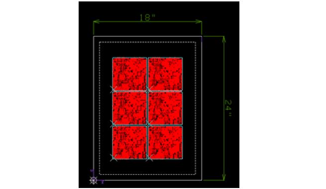
Fabrication panels are available in a variety of standard sizes to suit different production needs and PCB form factors. Common panel dimensions include 12 x 16 inches, 12 x 18 inches, 14 x 16 inches, 14 x 18 inches, 18 x 21 inches, 18 x 24 inches, and 21 x 24 inches, among others. Among these, the 18 x 24 inch panel is the most widely used size in the PCB fabrication industry due to its optimal balance of space utilization and compatibility with most production equipment. For applications that require larger PCB form factors, manufacturers also offer customized extended panel sizes, such as 21 x 32 inches, 30 x 30 inches, and even 30 x 40 inches. These extended sizes allow for high-volume production of large or complex boards, improving throughput and reducing material waste
Assembly Panel
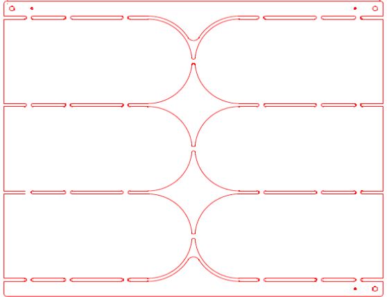
This panel is designed for the automatic component placement and soldering phases. Assembly panels also have features such as tooling holes, strips known as rail area on the outside edges for conveyor handling, and fiducial marks for pick-and-place alignment. These panels can also provide spacing between boards to avoid component collision during assembly. A Fab panel can have multiple assembly panels during the fabrication process.
When to make an Assembly Panel?
In PCB (Printed Circuit Board) manufacturing at Rush PCB Inc., especially for SMT (Surface Mount Technology) assembly, we often need two straight, opposite edges on the PCB that are free of components. These clean edges are important for the machines to grip and move the boards smoothly.
We usually create an assembly panel (also called an array) when:
- The board has an irregular shape
If the PCB is not a simple rectangle or square, it’s hard for the machines to handle it, so we put it in a regular-shaped panel. - The PCB is smaller than 4×4 inches
PCBs with a small form factor are difficult for machines to pick up and assemble, so multiple small boards are grouped into a larger panel. - The edge clearance is less than 200 mils (~5mm)
If components are placed too close to the PCB edges (where the machine grabs), we panelize to create safe gripping space. - It’s a mass production order
For big quantities, panels make the assembly faster and improve yield (fewer handling errors, better efficiency).
Features of the Assembly Panel

An assembly panel, or an assembly array, refers to a custom designed setup of several PCBs in an organized group for supporting automated assembly procedures like pick-and-place, soldering, inspection, and testing. These panels contain several structural and design aspects to promote efficiency, precision, and safety while assembling. Following are the most important features of an assembly panel.
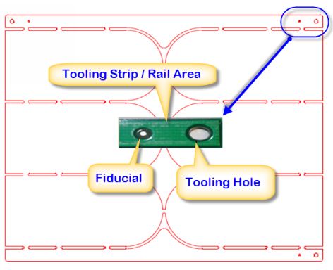
Tooling Strip/Rail area
Tooling strips, or rails, are attached to the outer edges of the panel. These areas of no function are used to support conveyor systems, fixtures, or clamping mechanisms during assembly. They may feature fiducials and tooling holes that are used to align the panel accurately within assembly machines. The width of this trip varies from 200 mil to 400 mil depending upon the edge overhang component placements.
Fiducials
Fiducials are copper pads placed on the rails (border areas) of the PCB array. They serve as reference points for automated pick-and-place machines, helping the equipment accurately align and position components during assembly. Typically, fiducials are 40 mils in diameter and should be left uncovered by solder mask to ensure clear visibility for the assembly cameras.
Tooling Holes
Tooling holes are non-plated holes placed on the rails (border areas) of the PCB array. Their purpose is to secure the panel during assembly by allowing it to be pinned down, which helps prevent unwanted shifting or movement. The standard diameter for tooling holes is 118 mils (approximately 3 mm), but they can be drilled to custom sizes based on specific requirements.
Whatever your PCB requirements, Rush PCB Inc. has your back. Contact us today for your free instant quote.


