How to Choose the Right SMD Component Package Size for Your PCB Design
Introduction
There are innumerable types of packages available for SMD components, which complicates the choice for the designer as to the specific size that would be the most suitable for their design. In this article, we, at Rush PCB Inc., will address this issue. We will discuss the several types of packages and the reason for their existence. We will also discuss the practical steps a designer must follow to effectively select the most optimum size that not only allows the board to function as intended but is also cost-effective for the project.
Electronic Components
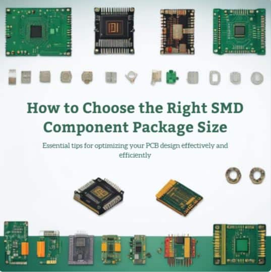
Electronic components available in the market are broadly of two types — Through Hole and Surface Mounted. Through hole components, identified by their long leads, require holes in the PCB through which the leads pass, to be soldered on the reverse side. Characterized by their larger size, through-hole components have been effectively superseded by surface-mounted components that offer several advantages.
SMDs or surface mount devices are relatively smaller and are characterized by the presence of tabs or tiny leads for soldering. In contrast to through hole components, SMDs do not require holes for mounting, requiring small pads on the same side on which to solder them. Being considerably smaller, it is easy to pack them closer on the board thereby achieving higher component density, resulting in smaller board sizes.
Size of Passive SMD Components
Due to the large variety of SMD components and their sizes, especially passive resistors and capacitors, the electronic industry uses a coding system to represent the components’ physical dimensions, both in imperial and metric units. Apart from deciding on the proper fitment of the components on a board, the codes are also a way of determining the components’ power-handling capabilities. The following table illustrates this for the most common sizes of SMD resistors and capacitors:
| Size Code | Approximate Size | Power Watt | Use Cases | ||||
| Inch | Metric | L (inch) | W (inch) | L (mm) | W (mm) | ||
| 008004 | 0201 | 0.010 | 0.005 | 0.250 | 0.125 | Mobile electronic devices, RF circuits | |
| 01005 | 0402 | 0.016 | 0.008 | 0.400 | 0.200 | ||
| 0201 | 0603 | 0.020 | 0.010 | 0.600 | 0.300 | 1/20 | |
| 0402 | 1005 | 0.040 | 0.020 | 1.000 | 0.500 | 1/16 | Consumer electronics, sensors |
| 0603 | 1608 | 0.060 | 0.030 | 1.600 | 0.800 | 1/10 | Various consumer, audio, and industrial devices |
| 0805 | 2012 | 0.080 | 0.050 | 2.000 | 1.250 | 1/8 | Power applications, LED drivers |
| 1008 | 2520 | 0.100 | 0.080 | 2.500 | 2.000 | ||
| 1206 | 3216 | 0.125 | 0.060 | 3.200 | 1.600 | 1/4 | High power and industrial applications, automotive applications |
| 1210 | 3225 | 0.125 | 0.100 | 3.200 | 2.500 | 1/2 | |
| 1806 | 4516 | 0.180 | 0.060 | 4.500 | 1.600 | ||
| 1812 | 4532 | 0.180 | 0.125 | 4.500 | 3.200 | 1 | |
| 1825 | 4564 | 0.180 | 0.250 | 4.500 | 6.400 | ||
| 2010 | 5025 | 0.200 | 0.100 | 5.000 | 2.500 | 3/4 | |
| 2512 | 6332 | 0.250 | 0.125 | 6.300 | 3.200 | 1 | |
Although small SMD components offer many advantages, they present challenges also. While the primary advantage is compactness and lightweight, the ultra-small components require specialized handling equipment for precise pick and place. Moreover, inspecting the tiny components is difficult, requiring high-power optical or X-ray systems.
Size of Active SMD Components
Like resistors and capacitors, active SMD components are also available in numerous types. The industry identifies them by prefixes, often followed by some numbers and letters providing additional information about the dimensions of the package, its pin count, or specific variations. The following table illustrates this for some common SMD packages:
| Prefix | Full Name | Description |
| SOT | Small Outline Transistor | Small SMD package with two or three leads |
| SOIC | Small Outline Integrated Circuit | Small SMD package with leads on two sides |
| QFP | Quad Flat Package | Square package with gull-wing leads on four sides |
| TQFP | Thin Quad Flat Package | A thinner version of QFP |
| LQFP | Low Profile Quad Flat Package | Thinner than QFP, but thicker than TQFP |
| BGA | Ball Grid Array | An array of solder balls on the bottom of the package for high-density connections |
| FBGA | Fine-Pitch Ball Grid Array | Smaller balls and tighter pitches than BGA |
| DFN | Dual Flat No-Lead | Small SMD package with no leads |
| QFN | Quad Flat No-Lead | Square package with terminals on four sides, no leads |
| CSP | Chip Scale Package | The package is as small as the die itself |
| WCSP | Wafer-Level Chip Scale Package | Extremely small package, nearly same as its wafer |
| LGA | Land Grid Array | Similar to the BGA package, but with flat contacts in place of balls |
| SOP | Small Outline Package | Rectangular package with gull-wing leads on two sides |
| TSOP | Thin Small Outline Package | A thinner version of SOP, mostly for memory chips |
Compared to the traditional through-hole packages, smaller packages like the SOIC or Small Outline Integrated Circuit, are a significant advantage, as they offer a thinner and more compact form factor. SOIC packages are rectangular with gull-wing leads on two sides, improving electrical performance as the shorter signal paths lead to reduced parasitic effects.
The TSOP or Thin Small Outline Package, being a variant of the SOIC design, offers more advantages, as it is even thinner. The lower profile is suitable for applications where the vertical space is limited.
For even higher pin density and versatility combined with a compact form factor, designers can consider QFPs or Quad Flat Packages and their variants like TQFP, LQFP, and QFN. The higher pin density comes from the package offering leads or terminals on all four sides.
For significantly higher pin density and compact form factor, BGA or Ball Grid Array packages offer several advantages. With solder balls on the underside of the package body, the shorter interconnects offer significantly higher electrical performance in terms of reduced parasitic capacitance and inductance. As their contact with the PCB is much higher compared to other package types, BGAs offer significantly better thermal performance. FBGAs or Fine-Pitch Ball Grid Array packages offer an even further increase in pin density and are suitable for modern mobile devices and other space-constrained applications.
Selecting the Right SMD Packages
After having looked at the myriad package types available from manufacturers of SMD packages, the designer rightly faces a dilemma in selecting the right package for their project. However, we provide a simple method, following which, the designer can easily choose the most optimum package. The key factors designers must consider, in sequence, when selecting SMD packages, are as follows:
- Power Dissipation — Resistors
Let’s face the truth; all electronic components exude heat, which is directly proportional to the product of the square of the current passing through it, and its internal resistance. If the current is of variable nature, it is usual to consider its RMS or Root Mean Square value for the calculation. Typically, the more heat the resistor must dissipate, the larger will be its size.
- Power Dissipation — Diodes and Transistors
For diodes and transistors operating in a linear mode, the heat generated is directly proportional to the product of the current passing through it, and the voltage across its terminals. For those operating in a switching mode, designers include an additional factor like the on-time ratio. Manufacturers publish an SOA graph depicting the Safe Operating Area for a transistor, which designers consult when selecting a transistor. Typically, the more heat the transistor must dissipate, the larger will be its size. Designers often use thermal aids like heat conducting substrates, thermal vias, and heat sinks to reduce the component size.
- Voltage Ratings for Resistors, Capacitors, and Transistors
Each of these components has a voltage rating that they can withstand without failing. Higher operating voltages typically mean larger package sizes together with larger spacing on the PCB. Designers use industry standards like the IPC-2221B, IPC-6012, and IPC-6018 for determining the appropriate spacing between conductive elements on their PCBs. Conforming to industry standards helps avoid the possibility of dielectric breakdown or corona discharges at high electric field strength, including the potential for dendritic growth or conductive anodic filamentation.
- Safety Factor and Derating
To be on the safer side, designers frequently apply a safety factor to their heat calculations. They typically derate the power handling capability of a component, and use components that can handle a somewhat higher power than what their circuits require. This helps to take care of situations where there is an inadvertent overloading on the circuit, allowing the circuit to continue operating without catastrophes.
- Signal Integrity
At higher operating frequencies, impedance mismatch, parasitic capacitance and inductance, and substrate absorption and dissipation play a significant role in degrading signal integrity. Designers must carefully assess switching speeds and operating frequencies, selecting components and substrates that match impedance needs. Selecting IC packages like BGAs and QFPs is of advantage here, as they can significantly reduce track length and parasitic elements. However, the designer must also consider the cost and complexity involved with these packages. For instance, using BGAs/FBGAs may mean increasing the number of layers in the PCB.
- Board Space
Depending on the application, the board size may require using miniature components, such as in mobiles and wearables. On the other hand, higher power handling may necessitate using larger components and a bigger board.
- Thermal Management
Designers may have to include external heat removal attachments to components where they cannot increase the package beyond a certain size. These could include larger pad sizes, larger thermal pads, or external heat sinks. While they must select a suitable package size, they must also allocate the necessary space for the heat sink on the board, and add holes/slots for fasteners.
- Cost
It may seem logical to go for miniaturization, as smaller components cost less. However, designers must also consider the challenges associated with miniature components. These could include changing to an assembler with a capable pick and place machine, a suitable solder paste printing machine, and a proper AOI/X-Ray setup. As handling miniature components is more challenging, the assembler may ask for more components to handle the rejections.
- Trade-Offs
Designers often have to trade off one advantage with another. For instance, although smaller package offers advantages like miniaturization and lower cost, they are more difficult to handle, and may pose difficulties in thermal management.
On the other hand, while larger packages offer easier manufacturing and better thermal management, they can take up larger space on the board, and cost more.
Designers, choosing between a BGA and a QFN package, may have to trade-off between:
- Simpler PCB design and easier inspection offered by the QFN but limited I/O count.
- Higher I/O density and better thermal performance of the BGA, but more complex assembly process and PCB design.
- Application Requirements
Frequently, the package type depends more on the application requirements. For instance, a wearable with limited space may require an FBGA to provide the intended functionality. On the other hand, automotive electronics require robust packaging with good thermal performance, so LQFP packages are more suitable.
Moving Forward
Manufacturers of SMDs are constantly pushing the boundaries in electronic design, going for increasing amounts of miniaturization, higher efficiency, and more power. Some new packaging trends in the industry are:
- WLP or Wafer Level Packaging — These integrate the IC at the wafer level, such that the final package is about the same size as the die itself, resulting in an ultra-compact form factor.
- 3D Packaging — By stacking multiple ICs vertically, manufacturers achieve significantly reduced footprints.
- Embedded Die Technology — It is now possible to embed the die directly onto the PCB, thereby achieving a significant increase in circuit density.
- FOWLP or Fan-Out Wafer-Level Packaging — This technology improves the fan-out of the traditional WLP by redistributing the connections, thereby providing a higher I/O count in a more compact package.
- MCM or Multi-Chip Modules — By combining multiple chips in a single package, MCMs reduce the overall footprint while improving system integration.
Conclusion
Modern electronic design depends critically on SMD or Surface Mount Device package types and their sizes. The availability of a diverse range of packages of both chip components and complex integrated systems offers substantial flexibility to designers in their quest for compact, efficient, and miniature electronic systems. We, at Rush PCB Inc., have tried to provide a cohesive understanding of the myriad SMD packages, tying together their characteristics for optimizing board space, performance, and thermal management.