This PCB assembly challenge involved attaching a solar panel to one side of a pad using solder paste with a pass through an SMT reflow soldering oven.

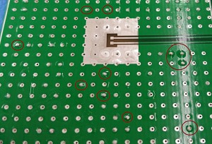
Solder wicking through the unmasked vias to the back side forms unacceptable “bumps” on top of the vias
The attachment or bond itself wasn’t the issue; but after the first trial runs, it was clear that solder wicking through the unmasked vias was going to be. Solder would wick through the unmasked vias to the back side and form “bumps” on top of the vias.
These bumps made the surface nonplanar and of course were unacceptable. It wasn’t an issue of using excess solder paste. But the “wicked wicking” had to be stopped, or at least prevented.
But how? Clearly, to keep the solder where we wanted it to remain during reflow, we had to find a way to prevent it from wicking up, collecting at the opposite ends of the vias and forming bumps. We had to find a solution that was simple, temporary, and tolerant of reflow soldering temperatures. The answer was Kapton polyimide tape, a familiar product to PCB assemblers for many years, and a material that does not degrade at reflow temperatures.

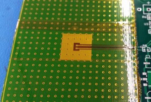
Kapton tape is applied to cover the unmasked vias; it will block the molten solder from leaking through.
Kapton tape was applied to cover the unmasked vias in order to block the molten solder from leaking through the vias to the back side during reflow. After reflow and cooling, it was a simple matter to peel off the tape. This temporary masking solution worked; there were no more solder bumps on the back side of the assembly, and the cost of the fix in terms of time and material was very low.

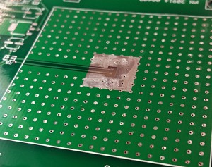
Figure 3. This temporary masking solution worked; there are no more solder bumps on the back side of the assembly.
Read about:FACTORS AFFECTING PRINT QUALITY OF SMT SOLDER PASTE


