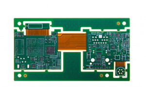
Rush PCB Inc. makes different types of flex and rigid flex PCBs starting from single sided to double sided, and multi-layered. These boards are special in the sense they can be bent either once, such as when they are being installed in a miniature camera, or bent multiple times such as when attached to the head of an inkjet printer.
Flex and rigid flex circuit board manufacturing has a fundamental difference from conventional PCBs in their use of basic material—this does not contain any glass reinforcement. Flexible circuits usually make use of various grades of Polyimide as their core or base dielectric. The Polyimide serves to provide both flexibility and mechanical integrity. On this Polyimide dielectric, a copper clad is bonded with a layer of adhesive called bondply (as against the conventional prepreg). After etching, this copper layer of traces is covered with a coverlay (similar to the conventional soldermask).
Flex and Rigid Flex Circuit Board Manufacturing
Circuit board manufacturers of flex and rigid flex start with the Polyimide base dielectric layer. Rush PCB Inc. uses Polyimides of various thicknesses from 12 µm to 125 µm, depending on the requirement. On this, they bond a rolled-annealed copper foil that can vary in thickness from 9 µm to 70 µm. Manufacturers use thermo-bond adhesives to bond the copper foil to the Polyimide base. These adhesives may include acrylic, phenolic butyral, and modified epoxy.
Panel Preparation
Fabricators first check the copper surface for imperfections such as dents and pits to ensure it meets the procurement standards. Usually, the manufacturer then bonds the copper sheets on to one or both sides of the Polyimide base using the adhesive in between. Application of heat and pressure in a lamination process makes the adhesive flow and bonds the copper foil to the Polyimide base.
As all the materials used are flexible in nature, handling techniques are crucial for the successful processing of flex circuits. Manufacturers modify their techniques and equipment adequately to support the thin laminates.
The fabricator then cuts down the full size sheets to usable panel sizes using shearing machines. Companies also use a standard fabrication panel size that fits optimally on all their production machines. Further processing of the panels begins with a baking process, which uses controlled heating for a defined period and a slow cooling process to remove moisture and helps to balance any internal stresses evenly.
Drilling
This stage begins by placing the panel between phenolic fiber boards to support it. Two or more registration holes along the edges of the panel serve to line up all the various features of the panel, including the drilled holes and the conductive pattern. The registration holes will also help in all stages of fabrication to align the panel on all the production machines at each step of the manufacturing process.
The registration holes help to align the panel on a numerically controlled drilling machine. The NC drill file supplied by the customer serves to program the drilling machine and to control the several heads with their corresponding tooling pins. The computer in the drilling machine moves the table to the proper location in both the x and y directions. The drilling head then picks the appropriate drill bit and creates holes in their programmed locations.
Also Read; Why RushPCB is the Leading PCB Manufacturer in USA
Through-Hole Plating
At this stage of circuit board manufacturing, the fabricator chemically deposits a very thin layer of electroless copper over the entire surface of the panel including on the inside of the holes. With the holes thus metalized, an electrical connection forms from one side of the flexible circuit to the other.
Imaging and Developing
The fabricator now prepares the panel for application of the conductive paste or circuit imaging. The surface preparation may consist of chemical dipping into an acid bath, followed by chemical cleaning, micro-etching, and application of an anti-tarnish agent.
Application of the image is usually accomplished by using a dry film, a screen printing process, or using a liquid photo imagable resist. The dry resist is laminated on to the panel using heat rollers. A sheet of film containing a negative image of the desired trace pattern is then placed on the coated panel.
Exposing the panel and the film to an ultraviolet light source hardens and fixes the specific areas of the resist under the transparent parts of the film, leaving the areas where the UV light does not penetrate as relatively soft and unexposed. The next stage is the developing process, where the unexposed soft resist is washed away, revealing the unwanted copper.
Also Read; How to Choose Professional PCB Prototype Assembler
The Etching Process
Fabricators use a chemical solution to dissolve the unwanted copper from the surface of the panel, leaving only the required copper circuitry under the photoresist. Once the hardened photoresist has been chemically stripped away, the desired copper pattern remains on the Polyimide surface.
An inspection process, involving visual and automatic optical inspection equipment, usually follows this stage. Sometimes, electrical test processes are also used.
Multilayer Rigid Flex Boards
Each additional layer is drilled and bonded on the base panel followed by the above process of through-hole plating, imaging, development, and etching. The fabricator bonds the rigid parts of the board also in the same manner.
Coverlay Application
At the final stage of the rigid flex circuit board manufacturing, the fabricator uses a coverlay to mask off all the copper areas of the flexible circuit that will not be soldered. This is an adhesive film prepared by drilling holes in the appropriate places, and the fabricator laminates this layer onto the flexible PCB.


