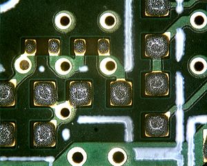
Importance Of Solder Paste Inspection
Unfortunately, in PCB manufacture there is always the risk of solder joint defects. It has been estimated that over half of all such defects are the result of improper solder paste printing. There are variations based on the print volume. For smaller volume printing, good solder paste printing practices can be acceptable. For larger printing volumes, it will be worthwhile considering using solder paste inspection (SPI).
When you think of the processes involved, surface mount assembly is complex. It relies on solder paste for connecting the leads on the integrated chip to the correct points on the board. The process involves using the stencil to print the paste onto the chip. This is then melted, resulting in a fused connection. There are crucial aspects of the process – the volume of solder used is vital in ensuring an effective fusing, as is the alignment. The complexity of achieving this has increased for two reasons – the density of components has increased in PCBs over time; and the SMT production often involves solder paste that is hidden from view.
Because of the technical issues involved, the solder printing process is responsible for the majority of assembly defects. As an example, if too much solder paste used; OR if too little is used, there is a risk of unreliable joints, leading to the risk of failure. Because of these risks, SPI was developed. It provides a tool that allows manufacturers to monitor the volume and alignment of solder paste, and can be integrated into manufacturer’s quality management systems.
The SPI process uses pictures taken from angle cameras that accurately measure the alignment and volume of solder paste. The pictures are then interpreted using software to provide key data about the printing process. The results help identify any potential errors that can then be addressed and corrected before assembly. SPI works to rapidly identify issues with volume or alignment of the solder. As a result, using SPI can improve the print quality and the yield, helping ensure efficient production of PCBs. The process also minimizes the potential of costs due to re-working of faults.
SPI was originally developed as a two dimensional tool, but has developed from 2D to 3D. The third dimension measures the height of the solder paste, enabling the equipment to accurately measure the volume that is being laid onto the board in the printing process. When 3D SPI is used in conjunction with Automated Optical Inspection, quality control can be ensured for both the placement of components and the associated placement of the solder print.
A sign of a good manufacturer is one who can provide PCBs on time, and defect-free. Manufacturers who integrate 3D SPI and Automated Optical Inspection have systems to ensure they can deliver your PCBs in line with your specifications. It will always be worth your while ensuring that you choose your manufacturer on this basis.


