

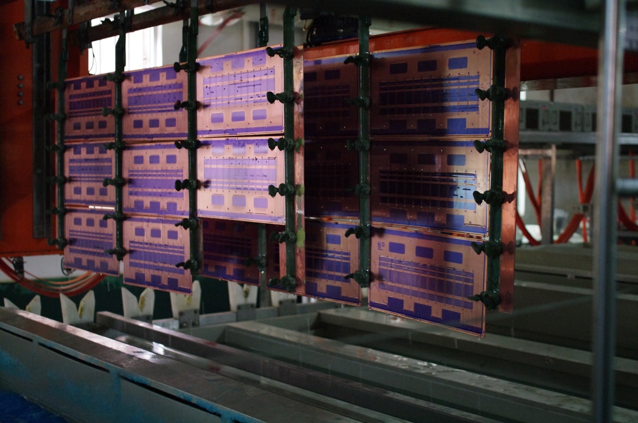
Rush PCB uses several ways of plating the exposed copper surface of a printed circuit board. However, the main function of any plating is to protect the copper from deteriorating, as any damage to copper tracks on a board will make it unfit for use. Another function of plating on a PCB is it helps to create a solderable surface while keeping the board safe when assembling it with components. Various options are available for PCB plating, and they have their pros and cons depending on the plating material underuse.
The PCB industry defines plating in two ways:
Via Plating
This is the process of filling a drilled hole with copper, with the aim of providing a reliable path for the current to flow. The current flows from the copper track on a board surface to another layer using the path provided by the via, and starts to flow onto copper tracks on the other layer.
Surface Finishing
This is process of covering the exposed copper surface of tracks on the top sides of the PCB. The plating helps to protect the copper on the outer surface of the PCB from damage because of exposure to moisture, contamination, oxidation, and environmental damage. In addition, it makes the copper surface more amenable to soldering.
Materials for Plating
Both via plating and surface plating strengthen the copper tracks on the PCB to allow better current flow. The next differentiation between plating comes from using various types of materials.
For via filling, only material that engineers use is copper. For surface finishing, however, they can use solder, silver, gold, nickel, and tin. The material they use for the plating depends on the application and the type of protection necessary. The various surface finishes commonly in use are:
HASL or Hot Air Solder Leveling
This type of surface plating uses solder to cover the copper. It is easy to apply, as the board only needs a dip in a molten solder bath. A hot air knife removes the excess solder from the surface. The process is economical and is popular.
HASL is easy to rework because it is adjustable. It also provides the PCB with the sturdiest plating finish. HASL suits SMT and through-hole component requirements. However, it makes the board thicker and heavier.
Immersion Tin
The immersion tin plating makes use of a chemical process to deposit a layer of flat metal (tin) on the copper traces. A major advantage of the immersion tin plating method is it does not involve using lead. Therefore, the process generates a PCB surface that is RoHS compliant.
Electroless Nickel Immersion Gold
This process deposits a thin layer of gold over a thin layer of nickel. The nickel layer acts as a barrier between the gold plating and copper. The gold layer helps to secure the nickel surface. However, the electroless nickel immersion gold plating process is expensive.
Immersion Silver
This plating process deposits a thin layer of silver over the copper traces. It involves dipping the printed circuit board into a solution containing silver ions. The best time for plating with immersion silver is during the PCB fabrication process, as it prevents the copper surface from oxidizing.
Electroplating
As the name suggests, this process uses electricity in a chemical solution where the PCB is one of the electrodes and the other electrode is a metal that will cover the copper tracks. The electric current guides and deposits the metal from the electrode into the solution and finally onto the copper surface. The metal electrode can be nickel, tin, or gold, depending on the plating necessary. The electroplating process is suitable for through-hole vias and surface copper traces.
Hard Gold
Hard gold plating, or electrolytic gold plating uses a thin gold covering on a nickel layer over the copper surface. The process produces a gold layer that is highly durable, and this makes the hard gold plating very common in the PCB industry. Although the presence of gold makes the process expensive, it offers a perfect surface for soldering.
Carbon Ink
As a highly robust surface finish, carbon ink provides a more affordable covering for copper tracks. Like the hard gold layer, a carbon ink also requires a nickel layer over the copper trace. However, compared to hard gold, carbon ink is less expensive.
Carbon coating on a PCB edge connector fingers provides a tough surface capable of withstanding several hundred insertions without damage. On push-button surfaces, the carbon ink coating easily withstands over a million operations. The viscosity and stability of carbon ink makes it eminently suitable for use in tropical applications.
Copper Plating
Engineers frequently use copper for plating copper traces and vias on a printed circuit board. The copper plating on the surface traces protects the pads from damage. But copper plating on the inner sides of a via or through hole helps provide a path for the current flow from one layer to another.
Creating vias may use the electroplating process or the electroless process. The electroplating process uses electricity and electrolysis, but the electroless process does not. Rather, the electroless process uses a catalyst in a chemical solution.
Various Styles of PCB Plating
Through hole plating
Just as for any PCB manufacturer, for Rush PCB also, through hole plating is a crucial process after drilling a PCB. The drill bit bores through copper and substrates in all the layers in the PCB. The drilling process produces heat, enough to melt the resin along the side of the hole. We use a low viscosity ink to produce a highly conductive film on the inner wall of the through hole, which dries after thermal curing. Now, fabricators can deposit copper on the inner wall directly by electroplating.
Brushing Plating
This plating procedure focuses on specific areas on the printed circuit board. The fabricator immerses a part of the board in the electrolyte. Therefore, plating takes place only on select parts of the board.
We use a chemically reactive anode such as graphite. We also wrap the anode with cotton or some other absorbent material. This allows plating selective areas of the board. Brushing plating is suitable for connectors on the board edges.
Reset Linkage Selective Plating
We apply this method of plating either automatically or manually. It produces a corrosion-resistant finish. The reset linkage selective plating, similar to brushing plating, is suitable for plating on selective areas of the board. Mostly suitable for coating gold fingers on board edge connectors, especially for flex PCBs, it increases the abrasive resistance of the fingers.
Conclusion
For Rush PCB, PCB plating is a vital process, especially during the fabrication of boards. It offers the best surface for the printed circuit board, increasing the durability and reliability of its traces and vias.


