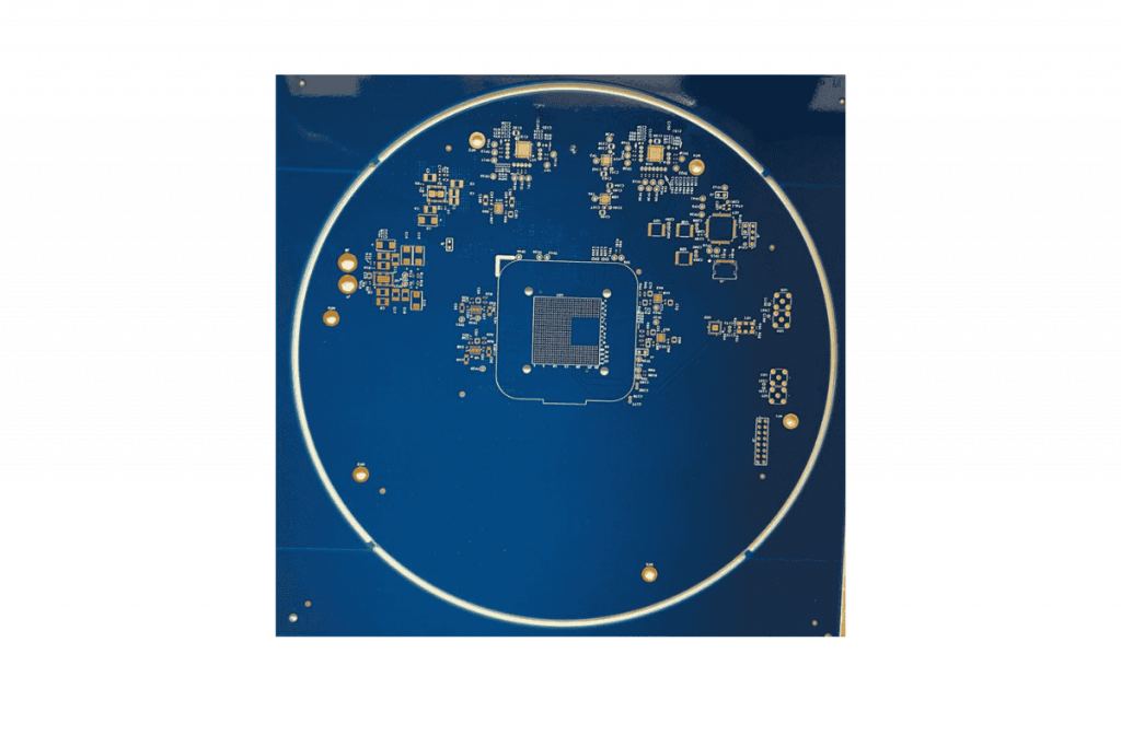
Electronic equipment typically uses PCBs or Printed Circuit Boards with some type of surface finish that not only protects the exposed copper surface of the board from oxidation but also prepares it for subsequent soldering of components. One such surface finish is ENIG or Electroless Nickel Immersion Gold.
At Rush PCB Inc., we manufacture PCBs with ENIG surface finish as it maintains the exposed copper pads as a reliable and robust surface for soldering. This is essential for electronic devices as it allows them to perform as intended for their lifetime. The electronic industry especially favors the ENIG surface finish as it offers excellent surface planarity, making the board suitable for mounting fine-pitch components. Moreover, ENIG is compatible with lead-free soldering processes, which are increasingly becoming acceptable owing to environmental regulations.
What is ENIG?
ENIG is a two-layer metallic coating finish, where the first layer is the Electroless Nickel and the second layer is Immersion Gold. Electroless nickel on the bare copper surface of the board acts as a barrier and a durable surface for soldering. The second layer of immersion gold acts as a protection layer to the nickel, protecting it during storage and also providing low-contact resistance. An ENIG surface finish is RoHS compliant.
Basics of ENIG
The ENIG surface plating on a PCB has two layers—electroless nickel covered with a thin layer of immersion gold—the nickel layer protecting the copper from oxidation, and the gold layer protecting the nickel from oxidation.
Compared to conventional surface finishes like HASL or Hot Air Solder Leveling, ENIG offers several advantages. These include:
- Excellent surface flatness (planarity)
- Suitable for mounting fine-pitch components

The ENIG Process
The ENIG process is complicated, involving multiple stages like cleaning the copper surface, activating it, depositing the nickel layer, and finally, immersing the board in a solution containing gold to form the final gold layer. It is necessary to understand each layer in detail.
The Electroless Nickel Layer
In an ENIG surface finish, the electroless nickel serves two purposes. First, it forms a barrier between the copper surface on the PCB substrate and the solder that binds the component to the board. This is essential as, during the soldering process, the exposed copper surface can easily oxidize, tarnish, and degrade, leading to poor solderability and potential failure of the board. The presence of nickel on the copper surface protects the copper from degradation.
Secondly, the presence of the nickel layer offers a robust and solderable surface on which to mount the electronic components. This is because nickel does not oxidize at the high temperatures of the soldering process, enabling the formation of a reliable solder junction to anchor the component to the board.
The Electroless Nickel Layer Plating Process
The process involving the electroless nickel layer plating has several steps. The PCB requires thorough cleaning and micro-etching to prepare the copper surface for the plating. The operator then immerses the board in a bath of nickel-phosphor alloy to deposit a thin layer of nickel onto the copper surface. Typically, the thickness of the nickel in the layer is between 3 and 7 micrometers, as this offers a good balance of cost, reliability, and performance.
The process of nickel deposition is electroless and autocatalytic, which means it occurs without the need for the application of external power. A chemical reducing agent in the bath reduces the nickel ions in the solution and deposits them onto the copper surface. The bath also contains small amounts of phosphorus, which co-deposits along with the nickel, and results in the layer actually being a nickel-phosphor alloy. We vary the phosphorus content between 2 and 14%, increasing the phosphorus content to make the layer more resistant to corrosion.
For an ENIG finish the quality and thickness of the nickel layer are critical. If the nickel layer is too thin, it can lead to solder joint failures and nickel corrosion. On the other hand, if this layer is too thick, the solder joints are likely to be brittle. To ensure a high-quality ENIG finish, it is necessary to control the plating process carefully.
The Immersion Gold Layer Plating Process
The immersion gold layer in the ENIG surface finish is basically for protection. It is a thin gold layer deposited over the nickel layer. In the final assembly process, the gold layer offers a low-resistance electrical contact.
The immersion gold process works as a displacement reaction. Gold ions present in the immersion bath displace nickel atoms at the top of the nickel layer. Being self-limiting, the process stops once a monolayer of gold atoms has completely covered the nickel surface. The final result is a very thin and uniform gold layer, with a typical thickness between 0.05 and 0.23 micrometers.
The operator immerses the PCB after nickel-plating in a bath containing gold ions, typically as a complex of gold cyanide. As the gold ions force out the nickel atoms on the surface, a thin layer of gold forms. Once the process completes, the operator rinses the PCB and dries it.
For the ENIG finish to perform properly, the quality of the gold layer is a critical factor. If the gold layer is thin or discontinuous, nickel can oxidize, leading to poor solderability. A thick gold layer, on the other hand, can lead to brittle solder joints. Therefore, just as for the nickel layer, it is also necessary to control the immersion gold process carefully thereby ensuring a high-quality ENIG finish.
Despite the thinness of the immersion gold layer, it plays a critical role in the reliability and performance of the ENIG finish. Not only does it protect the nickel layer from oxidation and provide a low-resistance electrical contact, but it also gives a pleasing golden appearance to the PCB.

Advantages of ENIG Surface Finish
The ENIG surface finish offers many advantages. Some of these advantages are:
- Uniform Surface Planarity — The excellent surface planarity of the ENIG finish makes the PCB particularly suitable for mounting fine-pitch components, which demand an extremely flat surface for proper electrical contact on all pins. The ENIG finish is substantially uniform and conducive to exceptional solderability, leading to reliable solder joints.
- Compatibility — ENIG is compatible with both leaded and lead-free solders. The versatility makes ENIG a suitable choice for all types of applications, ranging from consumer electronics to defense and aerospace systems. ENIG itself is RoHS compliant, but it can be used with leaded solders.
- Durability — By providing a robust barrier against oxidation, ENIG substantially boosts the durability of a PCB. While the nickel layer prevents the copper surface from oxidizing, the thin gold layer on it prevents the nickel from oxidation. This dual protection layer not only enhances the longevity of the PCB and also makes ENIG a suitable choice for applications requiring high durability.
- Longevity — One of the standout features of the ENIG surface finish is its longevity. The nickel layer, being hard and wear-resistant, withstands mechanical stress very well. Therefore, PCBs with ENIG finish are eminently suitable for connectors, BGA or Ball Grid Array assemblies, vias, and through-hole features operating in harsh environments. PCBs with ENIG surface finish have a long shelf life of more than 12 months. Although the gold layer in ENIG finish is only an atomic layer thick, it also provides excellent protection against corrosion. Being highly resistant to tarnishing and oxidation, the gold layer maintains the electrical performance of the PCB. This is especially important for applications where the board must perform in harsh environmental conditions, such as in outdoor or industrial applications. The electroless deposition process of the ENIG surface finish ensures continuous and uniform coverage of the copper surface, even when the geometry is complex. This further enhances the longevity of the PCB as all areas of the board remain adequately protected.
- Cost-Effective — PCBs with ENIG finish maintain their performance for long periods, even when working under challenging conditions. Their long lifespan makes ENIG one of the most cost-effective choices in the long run. Despite the higher upfront costs as compared to other surface finishes, ENIG is a popular and cost-effective surface finish for high-volume manufacturing.
- Superior Performance — The exceptional electrical conductivity offered by the gold layer in ENIG gives it an exceptionally high-performance advantage. This is a crucial factor for electronic devices, as high conductivity means there is minimal signal loss, necessary for high-frequency operations.
- Thermal Stability — As the nickel layer in the ENIG has a high melting point, PCBs with ENIG finish can withstand high temperatures during soldering and in operation. Thermal stability is a crucial factor in applications where the PCB faces high temperatures, such as in power electronic devices.
- Excellent Wetting — The combination of gold and nickel of the ENIG surface finish on copper offers excellent wetting properties, which translates into the formation of reliable solder joints. This feature is especially important for SMT or surface mount technology, as the quality of the solder joint impacts the reliability and performance of the assembled PCB.
Conclusion
When selecting a surface finish for a board, at Rush PCB Inc., we specifically consider the application requirements. After weighing the pros and cons of various finishes, we consider the unique characteristics of each finish and decide on the final one depending on its performance, cost, durability, and compatibility.
We use ENIG surface finish for PCBs due to the numerous advantages it offers, such as compatibility with other materials and processes, excellent surface planarity, and superior performance in terms of thermal stability, electrical conductivity, and solderability.
However, ENIG does have some disadvantages. These include higher upfront costs and the possibility of black pad formation.
FAQs
Can ENIG be used with both leaded and lead-free solders?
Compare ENIG with HASL regarding cost and performance.
How do you mitigate the black pad phenomenon?
Are there any disadvantages of the ENIG surface finish?
Why is ENIG so popular as a surface finish?


