

With the increasing demand for compact, lightweight, and high-reliability electronic products, flexible and rigid-flex PCBs have become essential in modern electronic design. These technologies enable dynamic, space-saving circuit layouts that are especially useful in applications like medical devices, wearables, aerospace systems, and consumer electronics. At Rush PCB Inc., we design flex and rigid-flex PCBs that are more complex than traditional rigid boards, particularly when it comes to manufacturability. To ensure a cost-effective, reliable, and high-yield product, engineers must follow Design for Manufacturability (DFM) guidelines tailored specifically to the unique characteristics of flex and rigid-flex technologies.
Material Selection
Guidelines
When designing flex and rigid-flex PCBs, it is essential to use materials specifically engineered for flexible applications. These include polyimide substrates, adhesiveless laminates, and coverlay films, which provide the necessary flexibility and thermal stability required in dynamic environments. In rigid sections, low-flow prepregs should be selected to prevent excess resin from flowing into adjacent flex areas during lamination. Additionally, all materials used in the construction of the PCB must comply with RoHS regulations and meet the necessary thermal and mechanical performance standards to ensure both reliability and regulatory adherence.
Bend Radius and Flexibility Considerations
Guidelines
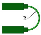
It is important to follow minimum bend radius guidelines to ensure the mechanical integrity and longevity of flex circuits. For single-layer flex designs, the bend radius should be at least six times the material thickness. In two-layer flex circuits, this increases to a minimum of ten times the thickness, and for multilayer flex circuits, a bend radius of twenty times the material thickness is recommended. These guidelines help prevent damage such as delamination, cracking, or trace breakage during bending.
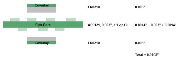
 Bend Radius (R) = 10 X 0.0108” = 0.1296”
Additionally, designers must consider the type of bending a flex circuit will undergo (Dynamic or Static). Dynamic bending involves repeated flexing during the product’s use, as in foldable or wearable devices, and needs stronger materials and careful design to handle continuous stress. Static bending happens only once during assembly, with little or no movement afterward. Each case requires proper material selection, trace layout, and support to ensure circuit reliability.
Avoid
Avoiding sharp bends and creases is essential in flex circuit design, as they create high stress points that can cause material fatigue, cracking, or delamination over time. Instead, smooth and gradual curves should be used in bend areas to distribute stress evenly and protect the flex material.
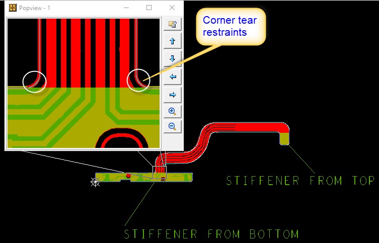
Furthermore, placing vias or pads within bend zones should be avoided, as they introduce rigid spots that are prone to failures like cracking, pad lifting, or open circuits. To ensure long-term reliability, these features should be kept in flat, unbent sections of the circuit.
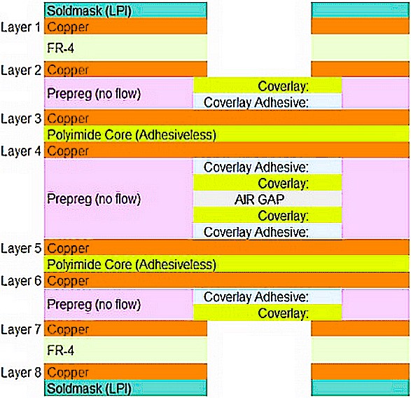
Stack-up Design
Guidelines
Clearly define the boundary between rigid and flex zones in your design to ensure proper material handling and fabrication.
Maintaining a symmetrical layer stack-up is also important, as it helps balance mechanical forces during manufacturing and reduces the risk of warping or twisting.
Avoid
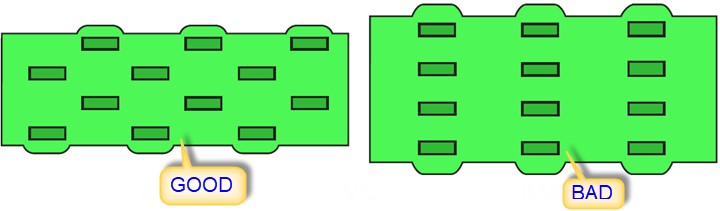
Avoid unbalanced copper distribution in the rigid sections of the PCB, as it can lead to bowing or twisting during the reflow soldering process. Uneven copper weights create thermal and mechanical stress imbalances, which may result in deformation, affecting both assembly and long-term reliability.
Trace Routing
Guidelines
To improve reliability in flex circuit design, Rush PCB Inc. recommends using curved or teardrop-shaped traces in bend areas to reduce stress concentration.

In multilayer flex PCB, where flexibility matters, avoid stacking traces of different layer over each other. Doing this will reduce the flexibility.
Traces should be routed perpendicular to the bend direction whenever possible, and consistent trace widths and spacing should be maintained to ensure stable impedance.
Avoid
Avoid using sharp corners, acute angles, or sudden direction changes in trace routing, as they can create stress points. Additionally, refrain from running parallel traces in bend areas, as they are more susceptible to delamination and cracking.
Coverlay and Solder Mask
Guidelines
In flexible PCB design, using a coverlay instead of a solder mask in flex zones is preferred, as it offers better mechanical protection and flexibility. Coverlay materials are more durable under bending stress, unlike solder masks that may crack or peel.
Avoid
Using traditional solder mask on flex areas is not recommended because it is brittle and prone to cracking. Flexible circuits undergo repeated bending, and solder masks are not designed to withstand such mechanical stress. This can lead to delamination or damage, compromising the reliability and performance of the flex PCB.
Via and Pad Design
Guidelines
In flex and rigid-flex PCB design, managing stress around interconnects is key to ensuring reliability. Pad reliefs and tear-drop vias help reduce stress where traces meet pads or vias by creating smoother transitions and lowering the chance of cracks.

Via-in-pad should be used only in rigid areas unless the flex manufacturer approves its use in flexible zones, as it can add stiffness and risk damage.
Also, unsupported pads in flex areas need mechanical backing to avoid issues like lifting or cracking during bending. Good design practices help maintain the circuit’s strength and performance.
Avoid
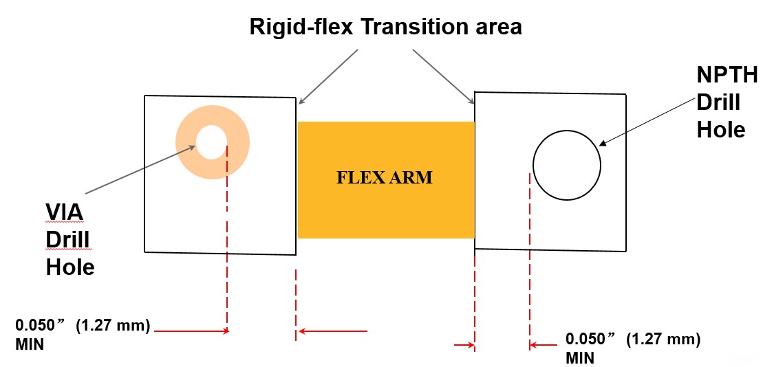
Avoid placing vias near the edge of flex regions or in bend zones, as they are prone to cracking or failure under stress. Instead, keep vias in flat, low-stress areas to maintain reliability.
Rigid-Flex Transition Zone
Guidelines
To improve mechanical reliability in PCB design, use fillets and gradual tapers in transition zones to spread out stress and reduce fracture risk. Also, include strain relief features like slots or cutouts to absorb stress from bending or temperature changes, helping to prevent cracks or damage—especially in flexible or high-stress boards.
Avoid
Avoid abrupt material changes or overlapping stiffeners without proper planning as it may cause stress points in PCBs leading to warping, delamination, or cracking, reducing durability and reliability.
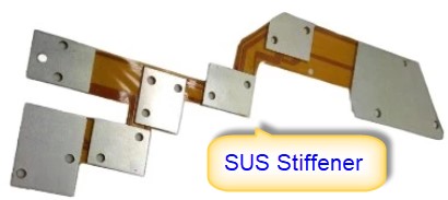
Stiffeners and Mechanical Features
Guidelines
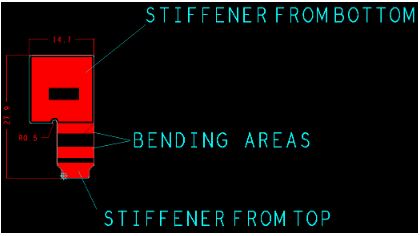
Use FR-4, stainless steel, or polyimide stiffeners to support areas where connectors or heavy components are mounted, ensuring durability and stability. These materials provide added mechanical strength to prevent board flexing or damage. When designing the stiffener outline, avoid sharp edges or corners. Smooth, rounded corners help distribute stress evenly and reduce the risk of cracking or failure.
Avoid
Avoid overlapping stiffeners with via arrays unless fully tested. Overlaps may cause mechanical or electrical issues. Test thoroughly if overlap is needed. This ensures reliable PCB performance.
Panelization and Assembly
Guidelines
Use breakaway tabs or tooling holes for easier handling and fixturing. Clearly mark flex regions on fab drawings to avoid damage. These steps improve manufacturing accuracy and protect flexible areas.
Avoid
Avoid placing components too close to bend areas to prevent stress damage. Minimize manual assembly by automating where possible to reduce errors. These practices enhance reliability and manufacturing consistency.
Communicate with Us
Flex and rigid-flex PCBs offer tremendous design freedom and performance benefits, but they demand close attention to manufacturability. RushPCB offers preferred solutions for high reliability rigid-flex PCB designs. We help our customers to design their flex and rigid-flex circuit boards to accomplish smaller bend requirements. We understand the challenges related to flex and rigid-flex design, fabrication, and assembly and deploy our expertise to eliminate concerns related to electrical instability, stiffness and via plating defects. By adhering to proven DFM guidelines, from material selection and stack-up design to trace routing and bend management. We help to avoid costly rework, delays, and product failures.
Through early collaboration with our customers, we, at Rush PCB Inc., translate your innovative designs into high-quality, producible circuits. So the most critical DFM step is to engage early with us as your PCB fabricator and assembler by providing following detailed documentation, including:
- Stack-up diagrams
- Material specifications
- Bend requirements
- Assembly constraints
- Acceptable tolerances
Our expert engineering can help optimize your design for both yield and performance.


