

Electronic systems use solder joints in multiple locations including connectors, components, and mechanical support points interconnecting printed circuit boards (PCBs). Rush PCB identifies system-level reliability as the dominant failure mode and isolates the critical location on the PCB as the most susceptible to failure. Accordingly, we list failure mechanisms in solder joints as occurring due to:
- Mechanical Loading—Overstress and Mechanical Fatigue
- Electrical Loading—Void formation in solder and Stress due to Current Flow
- Chemical Loading—Corrosion and Electro-Chemical Migration
- Thermal Loading—Overheating and Thermal Fatigue
Frequent Cause of Solder Joint Failure
According to Rush PCB, the most frequent cause of solder joint failure is thermo-mechanical fatigue, where mechanical loading along with thermal cycling leads to a synergetic damage process causing joint failure. The damage process may cause thermally induced mechanical strains in the joint or the solder alloy may undergo microstructural changes.
The industry uses different solder alloys, including Leaded and Lead-free ones, and these alloys have different microstructures responding in various ways to thermal loading. For instance, the industry’s most popular alloy group for board level reflow applications is the SnAgCu alloy, where the presence of Ag content in the alloy benefits shock/vibration durability and thermal cycling performance.
low Silver and low-melt Lead-free alloys
The industry also uses low Silver and low-melt Lead-free alloys. These are cheaper than SnAgCu alloys, and the low Silver presence allows the joint to be more robust to drops. Manufacturers often tailor such alloys by doping with Nickel and Bismuth to improve thermal cycling and drop reliability.
Why Good Solder Joints Fail
In general, the soft solder alloys that the electronic industry uses are rather weak, especially as joints operate at high temperatures relative to their melting point. However, the situation is more complicated, as information of shear and tensile strengths of solder alloys is not appropriate under real situations since creep and fatigue will influence the performance of the solder joint under actual loading conditions. Moreover, the presence of material defects also acts as a stress-raiser. That means, the printed circuit board with a normal solder joint cannot withstand a permanent mechanical load.
Solder alloys are sensitive to cyclic stress, while their capacity for load-carrying is low. This implies solder joints in the electronics industry have a finite life, leading to a finite life of the electronic equipment. Rush PCB recommends ensuring soldered joints have an appropriate lifetime for the application.
Corrosion: A Main Cause of Joint Failure
Although joints with proper soldering are adequately reliable for must purposes, the PCB may have several joints as potential failure sources due to inadequate design or doubtful processing. According to Rush PCB, there are three main causes for solder joints to fail:
- Fracture—tensile rupture from overloading
- Creep—long-lasting and permanent loading
- Fatigue—from cyclic loading
For most occasions, the above mechanisms work simultaneously, and there could be other causes as well, such as corrosion.
Joint Fracture from Short-Term Loading
Harsh treatment of PCBs or accidents often cause overloading leading to cracks developing in solder joints. For instance, when mounting a soldered assembly in position in its enclosure, the operator may use too much force, or when a user drops their mobile phone. In such cases, the shear stress on the solder joint exceeds its limit, resulting in a fracture of the joint.
Joint Fracture from Creep
Operating temperatures of the PCB higher than room temperature often cause creep, leading to solder joint fractures. For instance, a PCB after assembly and reflow soldering may have a rather large permanent warp, but its joints are relatively stress-free. When an operator mounts the PCB inside an enclosure and forces it to remain flat, the joints are subject to very large forces, eventually leading to cracks.
Joint Fracture from Fatigue
Temperature excursions accompanied by CTE mismatch is a major cause of joint fracture from fatigue. With typical cycle times measured in hours, the movements may be slow, but the deformation of the solder in the joint is rather large. Initial good joints may also succumb to this type of deformation and eventually crack.
Read About: MANUFACTURING PCBS FOR INDUSTRIAL BUSINESSES
Defective Solder Joints
Solder joints may also be defective due to inadequate process care. These may appear as:
- Disturbed joints
- Cold Joints
- Overheated Joints
- Joints with Insufficient Wetting
- Solder Starved Joints
- Solder Bridges
- Lifted Pads
- Stray Solder Splatters
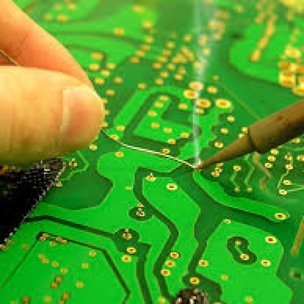
Disturbed joints are those subjected to movement as the solder was solidifying. The surface of the solder may appear to be rough, crystalline, or frosted. If one of the two surfaces was cold during soldering, the joint will not form and the result will be a cold and unreliable joint characterized by a lumpy and rough surface. Temperature plays a crucial part during soldering, and if the temperature is very high, the flux may vaporize before the solder has properly spread.
Read About: WHAT IS VAPOR PHASE REFLOW SOLDERING?
What Causes Older Wicking Down
Inadequate amount of solder present during soldering may not spread all over the surfaces totally, resulting in joints with insufficient wetting. Presence of an untented via or a through-hole very close to pad may result in solder wicking down the via and leaving very little for covering the pad, resulting in a solder starved joint. Excess solder present during soldering may result in solder bridges shorting neighboring pads. Other process related solder problems may cause lifted pads and stray solder splatters.
Prevention
As solder melts within a narrow specific temperature range, it is important to maintain this temperature in the oven for proper soldering. Cleaning the board and pre-heating it before the actual soldering helps to keep all surfaces at the right temperature for soldering.
Additionally, Adequate amount of solder deposit requires the use of a proper stencil. This ensures the pad has just the amount of solder it requires for complete wetting, but not enough to flow over to the next pad to cause a solder bridge.
Rush PCB has more than two decades of experience and expertise in manufacturing PCBs and assembling them. With sophisticated machinery at our disposal, we handle all types of PCBs with complete satisfaction of our customers. So, you can contact us for further queries.


