With semiconductor chip technology advancing by leaps and bounds, testing these dense and complex devices requires effective equipment to ensure their high functionality and reliability. By thoroughly testing them, chipmakers can ensure that their OEM customers remain confident that the products they are using are of the highest quality, and that their operations meet their specifications.
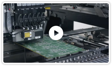
In view of the above, Rush PCB Inc offers high quality automated test equipment printed circuit boards or ATE PCBs to our customers. ATE PCBs serve as an effective interface to larger test systems. Major test activities require ATE PCBs for verifying chip functionality.
Using our ATE PCBs assures chipmakers about their chips functioning according to specifications, and they are ready to meet the new challenges from new requirements like handheld devices, wearables, Internet of Things, and more.
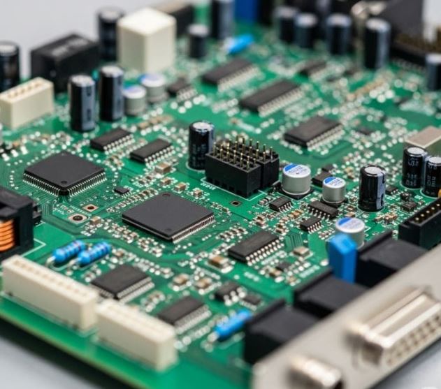
At Rush PCB Inc, we design, fabricate, and assemble ATE PCBs for testing a vast array of different semiconductor chips that include FPGAs or Field Programmable Gate Arrays, SoC or System on Chips, computer memories, microprocessors, and microcontrollers. However, we design, fabricate, and assemble an ATE PCB to test one specific type of chipset. Today’s chips are highly advanced and expensive, which makes it imperative to test them thoroughly for use.
Chipmakers require the chip-testing facility to be highly functional, and we have highly trained and experienced engineering personnel, and project managers to handle our ATE PCB fabrication and assembly. As ATE PCBs are far more complicated and sophisticated compared to conventional PCBs, the requirement for technical know-how and experienced personnel is also beyond the common level. Consequently, a successful assembly and testing of an ATE PCB helps to avoid considerable monetary loss, good-will loss, and loss of time-to-market for our customers.

Our Capabilities for ATE PCBs
At Rush PCB Inc, we invest in the latest and state-of-the-art tools, programs, and equipment. This ensures that we use short lead times for the test boards we fabricate and assemble, and they are cost-effective.
Our enhanced design and manufacturing capabilities ensure that our customers can avoid unnecessary delays that can be expensive for them.
We constantly upgrade our technology so that we are always ahead of our competitors for manufacturing ATE PCBs.
Why use ATE PCBs?
Reduced Testing Times
Testing complex semiconductor products manually is typically very time-consuming. Automated testing reduces the testing time drastically, without missing out any test procedure. Reduced testing times means our customers can reach the market faster, providing them a competitive advantage. ATE systems allow our customers not only the ability to improve their yield, but also reduce manufacturing costs.
Reduced Errors
Automated test equipment requires the operator to input data only once. Therefore, the chances of data input errors is reduced drastically. Moreover, as any unskilled person can input the data, utilization of skilled persons improves.
Consistency in Products
Automated test equipment bring consistency in testing products. That ensures the operator has not missed any test sequence, and there is consistency in products. As test equipment also have effective data management capabilities, it is possible to set qualifying limits that improve the statistical product reliability.
Who uses ATE PCBs?
Many industries use ATE PCBs for their ability to reduce test times and improve cost-effectiveness. This includes industries like:
- PCB assembly houses
- Semiconductor industries
- Component testing facilities
- Automotive industries
- Power electronic industries
- Consumer electronics industries
Why Rush PCB Inc. for ATE PCBs?
ATE PCBs must be robust and reliable. Small errors in ATE PCBs can result in humongous losses for the industry that uses them to test their boards. Industries rely on ATE PCBs from Rush PCB Inc. as they know they can rely on the boards to be robust, reliable, and trustworthy.
This is because we have the necessary talented and experienced personnel that can handle the design, fabrication, assembly, and testing of ATE PCBs and the programs that make these boards effective. Unlike personnel for conventional PCBs, our special team for ATE PCBs can:
Understand and handle non-conventional illustrations, diagrams, and circuits. For instance, apart from the conventional netlist, ATE PCB designers must understand and handle ball maps, bit maps, and map drawings.
Understand and handle digital and analog hardware and software exclusive to the ATE PCB technology.
Exclusively handle the sophisticated assembly processes involved with ATE PCBs.
How are ATE PCBs Different?
Compared to conventional PCBs, ATE PCBs are a lot different. Their difference is in the:
- Size of the board—ATE PCBs are large, 20-inch x 22-inch to 24-inch x 30-inch.
- Number of Layers—Depending on the complexity, the boards can have 40 to 60 layers, with a considerable number of ground and power planes.
- Extra processing required—Because of the high number of layers, and the presence of many ground and power planes, the ATE PCB requires more heat and pressure during its formation. It also requires a highly specific thermal profile to solder the components on the board, as it requires considerable amount of heat.
- Special Stencil Design—Proper. Precise stencil design forms the linchpin of the ATE PCB assembly, and this is extremely important.
Handling the above requirements needs personnel with the requisite knowledge and experience. Our expert team can join hands with you to give you an edge in building your ATE PCB.
We offer unparalleled quick turnaround times. Let us know your requirements, and we can build ATE PCB prototypes for you and assemble them in 24 hours. Get in touch with us today with your requirements, and we will get back to you with a quick quote.