

Rush PCB Inc. makes High-Density Interconnect (HDI) Printed Circuit Boards (PCBs), which are essential for modern electronic devices that require compact and high performance circuitry. A defining feature of HDI technology is the use of advanced via structures to achieve interconnectivity across multiple layers of the PCB without increasing size or compromising performance.
Via is a complex 3D structure. Its use not only impacts the integrity of the signal but the cost of the PCB as well. Higher the number of vias, higher the cost. There are many different types of vias and they can be drilled using different technologies. The type of the via and the technologies adapted to define those vias on the PCB, also impacts the cost of the fabrication. Some vias are costlier to manufacture than the others. At RushPCB we have not only mastered these sciences not only from a manufacturing point of view but we help our customers decide the types of vias required for their design. We study the design complexity, the performance parameters of the product and the speed of the signals on the PCB to choose the right set of vias for the PCB. In this article we shall explore the types of vias used in HDI PCBs and compare the most common via fabrication methods, including laser drilling, mechanical drilling, and emerging alternatives.
Types of Vias Used in HDI PCBs
HDI PCBs employ a variety of via types, each designed to meet specific layout and performance requirements:
- Through-Hole Vias
- Blind Vias
- Buried Vias
- Microvias
- Skip Layer Laser Vias
- Via-in-Pad (VIP)
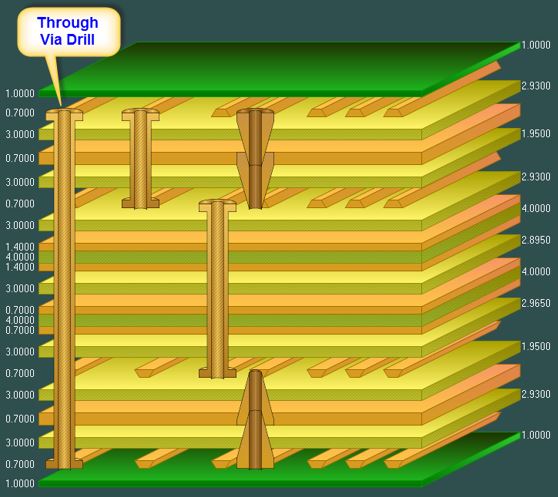
Through-Hole Vias
Through hole vias are the most traditional type used in PCB design, extending from the top to the bottom layer. They are mechanically drilled and copper plated to connect all layers they pass through. Aspect ratio (board thickness divided by smallest via hole diameter) is critical, with 10:1 being the industry standard. For example, a 1.6 mm board needs a 0.2 mm hole. Today, aspect ratios up to 20:1 are possible for holes 10 mil and above, but higher ratios can cause plating defects and reduce reliability. These vias block routing paths across layers, limiting signal density, which leads designers to prefer microvias.
Blind Vias
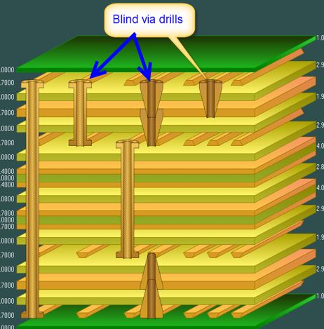
Blind vias connect an outer layer (top or bottom) to adjacent inner layers without going through the entire board, making them “blind” from the opposite side. By connecting only specific layers, they free up space on deeper layers, improving routing efficiency and allowing higher component density—ideal for compact, multilayer designs. Like through-hole vias, blind vias must maintain an aspect ratio, typically 0.75:1, for reliable copper plating, though ratios up to 1:1 are possible.
Buried Vias

Buried vias connect only internal layers of a multilayer PCB and are hidden from both top and bottom surfaces. They enable internal interconnections without affecting surface routing or components. This increases routing density and design flexibility, especially in complex HDI designs where space is limited. Buried vias require sequential lamination, making the process more complex and costly, but essential for high performance multilayer stack-ups. Since they are inaccessible after lamination, rework is not possible, so high manufacturing precision is crucial.
Microvias
Microvias are ultra-small vias, typically 20-150 µm in diameter, designed to connect adjacent layers in a multilayer PCB. Unlike through-hole or buried vias, microvias are used in high-density layouts where space savings and precision are essential.
Microvias are almost always created using laser drilling, which provides the precision needed to form such small, clean holes in thin dielectric materials. They’re usually used in blind configurations (from the outer layer to the next), and in some cases, stacked or staggered to connect multiple internal layers.
Microvias can be used in different configurations depending on how many layers need to be connected and the mechanical reliability required. These configurations are a key part of HDI PCB design. Listed below are different configurations of micro vias:
Single Layer Microvias
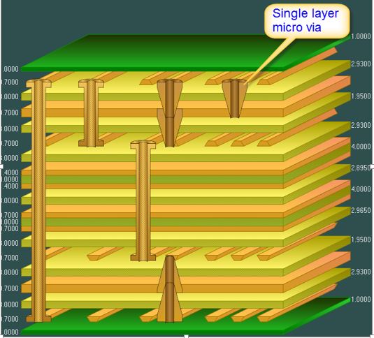
A single layer microvias connects only two adjacent layer e.g L1 with L2. This is most common and simplest form of microvias and ideal for saving space and improving signal performance.
Stacked Microvias
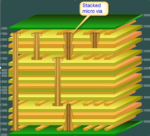
Multiple microvias are vertically aligned on top of one another to span several layers. They are used when connections must go deeper than two layers. It requires careful processing to ensure strong via to via adhesion and plating reliability.
Staggered Microvias
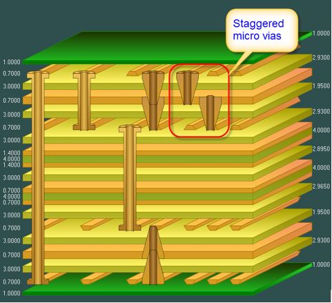
In this type, microvias are offset from each other across multiple layers, avoiding direct vertical alignment. This formation reduces mechanical stress and improves reliability especially in high thermal or flex environments. As compared to stacked vias, this technique is slightly more complex to route but mechanically more robust.
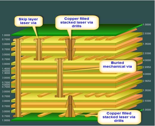
Skip Layer Laser Vias
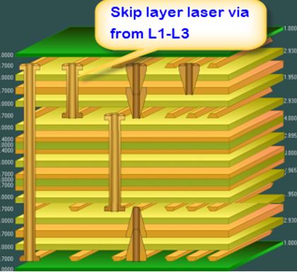
Skip layer laser vias are laser-drilled microvias that connect non-adjacent layers in a multilayer PCB, skipping one or more internal layers. Unlike standard microvias, which link only adjacent layers, skip layer vias provide direct electrical connections between layers separated by intermediate ones. This improves signal integrity by reducing vias and interconnects signals must cross, minimizing loss and interference. It also simplifies routing and saves PCB space, allowing higher component density. Additionally, we, at Rush PCB Inc., use skip layer vias to enhance design flexibility for complex multilayer and HDI PCBs, improving electrical performance through shorter, more efficient paths.
Via-in-Pad (VIP)
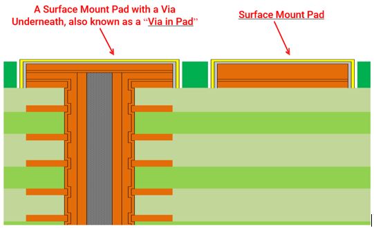
A via-in-pad microvia is placed directly under a component pad, often beneath fine-pitch BGAs, QFNs, or flip-chip packages. Unlike standard vias outside pads, these allow ultra-compact layouts by embedding vias where the component lands. This saves board space, improves thermal dissipation through internal copper layers, and enhances electrical performance by shortening interconnect paths. However, challenges include solder wicking during reflow and voiding that affect reliability. To address these, via-in-pad microvias are usually filled with epoxy and plated over to create a flat, solderable surface, requiring careful fabrication and assembly control.
Comparison of Drilling Methods
Laser Drilling
Laser drilling is the most widely used method for creating microvias, especially in HDI applications. Laser systems can drill vias as small as 20 µm in diameter, making them ideal for ultra-fine-pitch components and high-density interconnects where mechanical drilling simply can’t reach. Unlike mechanical drills, lasers can be finely tuned to stop at a specific layer, making them perfect for creating blind and stacked microvias without damaging adjacent layers. This control is essential in HDI builds that use sequential lamination and multiple via structures.
Despite of above stated Pros, laser drilling is expensive as compared to mechanical drilling and it is sensitive to material composition.
Mechanical Drilling
Mechanical drilling is the traditional method for creating vias in PCBs, using high-speed rotating drill bits to bore through the substrate. It’s suitable for larger vias (typically >150 µm) and cost-effective for high-volume production where fine pitch isn’t critical. Mechanical drilling is used for through-hole, blind, and buried vias. However, it can’t achieve small diameters needed for HDI designs, and drill bits wear out over time, affecting hole quality. It also causes mechanical stress, especially in high-aspect-ratio or multilayer boards, which can impact reliability
Other Drilling Methods
Plasma Etching
Plasma drilling, or plasma etching, is a non-mechanical chemical process that uses ionized gas to remove material and form vias. It’s useful when mechanical or laser methods may be too harsh. The PCB is exposed to reactive plasma that chemically etches the substrate at specific spots, ideal for delicate or flexible materials. Mainly used in flex and rigid/flex PCBs, it avoids mechanical strain. However, plasma etching is slower and less precise than laser drilling and unsuitable for very small microvias or mass production.
Focused Ion Beam (FIB) Drilling
Focused Ion Beam (FIB) drilling uses a focused ion beam, typically gallium, to sputter material and create micro-scale features like vias or cuts. It’s mainly used in R&D, prototyping, and failure analysis, allowing precise modifications at micron or sub-micron levels. FIB offers exceptional control for targeted rework and defect isolation without affecting nearby areas, also aiding cross-sectioning and imaging. However, it’s slow, costly, and not suitable for mass production, making it ideal for research and failure analysis rather than volume manufacturing.
Comparison Table
| Feature | Laser drilling | Mechanical Drilling | Plasma/FIB/Other |
| Via Types Supported | Microvia, Blind, VIP | Through-hole, Blind | Microvia (flex/R&D) |
| Minimum Via Size | ~20 µm | ~150 µm | <20 µm (FIB) |
| Speed | High | Medium to High | Low |
| Equipment Cost | High | Low | High (FIB), Medium (Plasma) |
| Material Compatibility | Selective | Broad | Depends on method |
| Typical Use Case | HDI, mobile devices | Standard multilayer PCBs | Flexible PCBs, prototyping |
Summary
At Rush PCB Inc., we use advanced via technologies as they play a key role in HDI (High-Density Interconnect) PCB design. As electronic devices become smaller and more powerful, choosing the right via type and drilling method is more important than ever. Microvias, usually created by laser drilling, are vital for high-speed and space-saving designs. Blind and buried vias help route signals efficiently in multilayer boards. Mechanical drilling is still useful for standard or budget-friendly projects. Other specialized methods are used for flexible circuits and advanced prototypes. By understanding the strengths and limitations of each via type and drilling technique, designers can achieve better performance, lower costs, and reliable manufacturing.


