


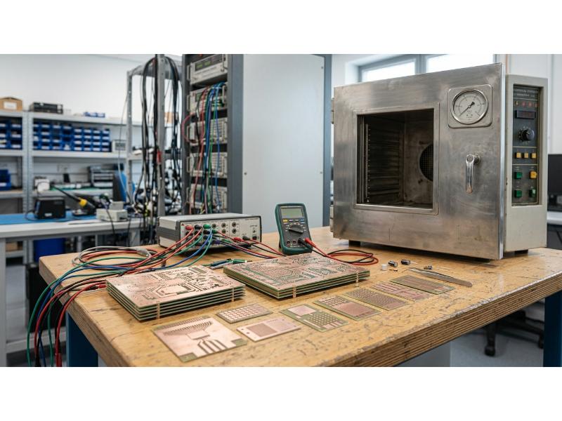
Printed circuit boards (PCBs) are exposed to a wide range of temperature conditions during manufacturing, assembly, testing, transportation, and normal operation. Repeated heating and cooling can produce mechanical stresses within the PCB because the different materials used in its construction do not expand and contract at the same rate. A multilayer PCB typically consists of copper, resin, glass fibers, solder mask, surface finishes, and other dielectric materials, each having different thermal expansion characteristics. These differences can create mechanical stress when the PCB experiences rapid or repeated temperature changes. Thermal stress testing is therefore an important reliability test used to evaluate how a PCB and its interconnections withstand elevated temperatures, thermal cycling, and other temperature-related stresses. The test can reveal weaknesses such as plated-through-hole barrel cracking, delamination, pad separation, copper cracking, solder-joint failure, and other structural defects. Thermal stress testing is especially important for high-reliability PCBs used in automotive, aerospace, industrial, telecommunications, medical, and power-electronic applications, where long-term exposure to temperature variations can significantly affect product reliability. At Rush PCB Inc, we perform rigorous thermal stress testing to help manufacturers improve materials, manufacturing processes, design margins, and overall product quality before boards reach the field.
What Is PCB Thermal Stress Testing?
A thermal stress test for PCB aims to check the actual bearing capacity of finished printed circuit boards against regular temperature changes. Thermal stress tested for PCB can expose hidden structural weak points that ordinary electrical performance checks cannot find, and these hidden issues will gradually trigger equipment breakdowns in actual working scenes.
Different raw materials used in PCB production such as copper foil insulating base material and protective solder mask all feature distinct expansion and shrinkage degrees when temperature rises or drops. Long term temperature changes will generate strong shear force on the joint positions of different materials including inner board connecting holes and surface welding areas. The whole set of thermal stress test for PCB work adopts controllable repeated temperature change modes to speed up the appearance of such structural damages, so production teams can finish quality confirmation before formal mass production.
Why Thermal Stress Occurs in PCBs?
The primary reason thermal stress develops in a PCB is the difference in the coefficient of thermal expansion (CTE) of its constituent materials. CTE describes how much a material changes in dimensions when its temperature changes.
Copper, resin, glass reinforcement, and other PCB materials have different thermal expansion characteristics. When the temperature increases, each material attempts to expand according to its own CTE. Because these materials are bonded together, they cannot always expand independently. Mechanical stresses therefore develop at interfaces and within the PCB structure.
The effect becomes particularly important in the Z-axis, or thickness direction, of a multilayer PCB. Resin-rich dielectric materials can exhibit greater thermal expansion in the Z-axis than copper. During heating, the dielectric material may expand more than the copper plating inside a through-hole. This difference places stress on the plated copper barrel.
Repeated heating and cooling can eventually produce fatigue damage, particularly when the PCB contains manufacturing defects or insufficient structural margins.
Thermal Expansion in the Z-Axis
Z-axis thermal expansion is especially important for plated-through-hole reliability. A plated-through hole contains a copper barrel extending through the thickness of the PCB. During heating, the dielectric material surrounding the barrel can expand in the Z direction.
If the dielectric material expands more than the copper barrel can accommodate, mechanical stress develops in the plated copper. During cooling, the materials contract again. Repeated thermal cycles can cause fatigue in the copper plating.
If the copper plating is too thin, contains voids, has poor adhesion, or has other defects, repeated thermal stress can eventually produce a crack. Such cracking may lead to intermittent electrical connections or complete electrical opens.
For this reason, thermal stress testing is widely used to evaluate the integrity of plated-through-hole structures.
Thermal Stress During PCB Manufacturing
Thermal stress does not occur only during the operational life of a PCB. The board experiences several high-temperature processes during manufacturing and assembly.
During multilayer lamination, the PCB stack-up is exposed to elevated temperature and pressure. During soldering, the board may experience temperatures significantly above normal operating conditions. Lead-free solder assembly can impose particularly demanding thermal conditions because lead-free soldering processes generally operate at higher temperatures than traditional tin-lead processes. Additional thermal exposure may occur during rework, repair, component replacement, and multiple assembly passes. Therefore, a PCB may experience several thermal excursions before it is even placed into its final application.
A properly designed and manufactured PCB must tolerate these manufacturing-related thermal stresses without delamination, cracking, or loss of electrical integrity.
Test Specimens and Coupons
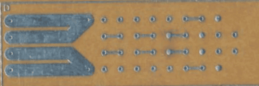
Thermal stress testing can be performed on complete PCBs, representative test vehicles, or specially designed test coupons. Coupons are useful because they can contain representative plated-through holes, vias, layer constructions, and material combinations without requiring destructive testing of an entire production board.
A thermal stress coupon may contain multiple hole sizes and plating structures designed to represent critical features of the production PCB. After testing, selected holes can be evaluated using electrical measurements and microsection analysis.
Using coupons allows manufacturers to monitor process reliability without sacrificing large numbers of finished boards.
Typical Thermal Stress Test Procedure
The exact thermal stress procedure depends on the applicable product specification, customer requirement, PCB construction, and qualification standard. A general procedure begins with selecting representative test specimens and establishing their initial condition.
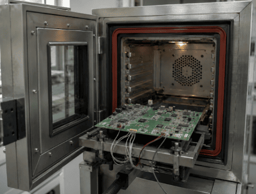
The specimens are then exposed to the specified thermal environment. For a thermal cycling test, the boards are repeatedly moved between defined temperature limits. The number of cycles and dwell times are controlled according to the applicable test requirement.
After the required thermal exposure, the specimens are inspected for physical and electrical degradation. Electrical resistance measurements may be taken before, during, or after testing depending on the test method. Selected samples may then undergo microsection analysis to identify cracks or other internal defects.
It is important that actual test parameters be taken from the applicable specification rather than using generic temperature and cycle values, because requirements can vary according to the PCB type and qualification program.
Plated-Through-Hole Reliability
One of the primary objectives of PCB thermal stress testing is evaluating plated-through-hole (PTH) reliability. A PTH creates an electrical connection between different PCB layers through a copper-plated hole.
During thermal exposure, the dielectric material surrounding the PTH expands and contracts. Because the copper barrel and dielectric material have different thermal expansion characteristics, mechanical stress develops in the barrel.
Repeated cycling can result in barrel cracking, especially near areas where the copper plating experiences concentrated stress. If a crack extends through the copper barrel, the electrical connection may become intermittent or completely open.
Thermal stress testing therefore provides valuable information about the quality of the drilling, desmear, electroless copper, electroplating, and lamination processes.
Copper Plating Quality
Copper plating quality has a significant influence on thermal reliability. The copper deposited inside a drilled hole must have sufficient thickness, uniformity, ductility, and adhesion to withstand thermal expansion and contraction.
A plating layer containing voids, cracks, inclusions, excessive roughness, or insufficient thickness may be more vulnerable to thermal fatigue. A well-controlled plating process produces a more robust hole wall capable of accommodating repeated thermal stress.
For high-reliability PCBs, microsection analysis can be used to verify plating thickness and identify defects that could contribute to thermal failure.
Delamination and Thermal Stress
Thermal stress can also cause or reveal delamination within a PCB. Delamination refers to separation between layers or interfaces within the board structure.
Poor bonding, moisture absorption, contamination, inadequate lamination parameters, inappropriate resin systems, or excessive thermal exposure can contribute to delamination. When the PCB is heated, trapped moisture can also expand and increase internal pressure.
Thermal stress testing can therefore reveal weaknesses in the bond between copper and dielectric materials or between different dielectric layers. Delamination may appear as internal separation, blistering, or localized material damage.
Solder Joint and Component Stress
Thermal cycling affects not only the PCB itself but also the solder joints connecting electronic components to the board. Components and PCB materials can have different thermal expansion characteristics, causing relative movement during temperature changes.
Large components can generate significant mechanical stress because their thermal expansion may differ from that of the PCB. Fine-pitch packages, BGAs, power components, and other large or mechanically constrained devices may therefore require careful thermal-reliability evaluation.
For assembled PCBs, thermal cycling can be used to evaluate the combined reliability of the PCB, solder joints, component packages, and interconnection structures.
Detection of Thermal Stress Failures
Thermal stress failures can be detected through several inspection methods. Electrical resistance testing can identify changes in the continuity of plated-through holes or other interconnections. An increase in resistance or a complete open circuit may indicate damage to the conductive structure.
Microsection analysis is one of the most useful methods for identifying internal thermal failures. A cross-section can reveal barrel cracks, corner cracks, separation, plating defects, delamination, and other structural abnormalities.
X-ray inspection can also be useful for examining internal structures without completely destroying the test specimen. For assembled boards, X-ray inspection may help identify certain internal defects associated with components and solder joints.
Common Thermal Stress Failures
Thermal stress testing reveals several failure modes that compromise PCB reliability. Understanding these helps engineers design more robust boards.
Solder Joint Fatigue:
Repeated thermal cycling causes stress concentration at solder ball interfaces, leading to micro-cracks or open circuits. A 2022 study noted that lead-free SAC305 solder joints failed after 1,500 cycles between -40°C and +125°C due to fatigue.
Via and PTH Cracking:
CTE mismatches between copper plating and substrate materials can fracture vias or PTHs, especially under thermal shock. High-aspect-ratio vias are particularly vulnerable, with failure rates increasing by 20% in rapid temperature shifts.
Delamination:
Extreme heat can cause separation between laminate layers, weakening the PCB’s structural integrity. This is common in low-Tg substrates exposed to temperatures above 150°C.
Component Failure:
Thermally induced stresses, like electromigration in ICs, can cause immediate or long-term component failures, reducing PCB lifespan.
By identifying these issues early, engineers can adjust materials, layouts, or manufacturing processes to enhance reliability.
Prevention of Thermal Stress Failures
Preventing thermal failures begins with selecting appropriate PCB materials. Laminate systems should have thermal and mechanical properties suitable for the expected application and assembly process.
Manufacturing processes must also be controlled. Proper lamination, drilling, desmear, electroless copper deposition, electroplating, and curing are essential for creating robust interconnections.
Adequate copper plating thickness and good hole-wall quality are particularly important for PTH reliability. Designers can also improve thermal reliability by selecting appropriate hole sizes, aspect ratios, pad geometries, and layer constructions.
Conclusion
PCB thermal stress testing is an important reliability evaluation used to determine whether printed circuit boards and their interconnections can withstand the thermal conditions encountered during manufacturing and service. Differences in thermal expansion between copper, resin, glass reinforcement, and other materials can create mechanical stresses, particularly in multilayer structures and plated-through holes.
Repeated thermal cycling can gradually produce fatigue in copper plating, leading to barrel cracking, corner cracking, delamination, and electrical failure. The risk becomes greater when the PCB contains inadequate plating thickness, poor adhesion, material instability, excessive moisture, or manufacturing defects.
Effective thermal reliability requires a combination of appropriate material selection, controlled lamination, accurate drilling, high-quality copper plating, suitable PCB design, and reliable inspection. Thermal stress testing, together with electrical testing and microsection analysis, provides manufacturers with valuable information about the structural integrity and long-term reliability of PCB constructions.
For high-reliability electronics, thermal stress testing should be considered an important part of the PCB qualification and process-control strategy. Companies like Rush PCB Inc help identify thermal weaknesses before products reach the field, allowing manufacturers to improve PCB reliability, reduce failure rates, and ensure that the final product performs consistently throughout its intended service life.


