


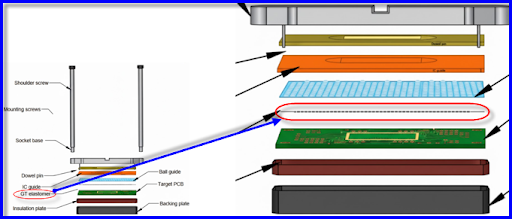
Ball Grid Array (BGA) technology dominates advanced electronics due to its compact form factor and high I/O density. While BGAs are normally soldered directly to the PCB, many applications require a socket BGA. These sockets allow components to be mounted, removed, and replaced without soldering. They are widely used in prototyping, validation, burn-in testing, and mission-critical systems where serviceability or frequent device swapping is necessary.
At RUSH PCB Inc, we understand that the reliability of a socket BGA assembly depends on three primary factors:
- The contact mechanism that connects the package balls to the PCB pads.
- The solder mask design of the pad layout on the PCB.
- The surface finish applied to the PCB pads for durability and signal integrity.
This article examines each of these areas in detail, outlining the requirements and trade-offs that designers must consider.
Types of Contact Mechanisms
The defining feature of a socket BGA is its contact system. Unlike soldered BGAs, which rely on solid solder joints, sockets must maintain reliable mechanical pressure and low contact resistance through multiple insertions. Here are the main mechanisms that are commonly used:
- Sockets with Spring Loaded Pin Contacts
- Sockets with Conductive Elastomers
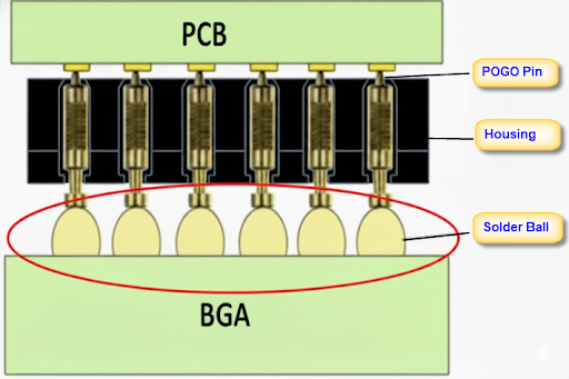
Sockets with Spring Loaded Pogo Pin Contacts:
The design uses spring-loaded probes that aligns accurately with each BGA ball. This approach offers several advantages, including high durability with the ability to withstand tens of thousands of insertion cycles, stable electrical performance with low contact resistance and suitability for burn-in and test socket applications.
However, this design also has some limitations. It tends to be relatively expensive and requires a larger footprint, making it difficult to use for pitches below 0.5 mm. Moreover, the use of pogo pins or spring-loaded probes can introduce extra inductance, which may impact the performance of very high-speed signals.
Sockets with Conductive Elastomers:
This design uses conductive elastomer strips or dots embedded within a silicone matrix. Each elastomer column forms an electrical bridge between the BGA ball and the PCB pad when compressed. It offers several advantages, including a very low profile that makes it ideal for thin systems, low inductance and capacitance that enable excellent high-frequency performance, and a simple assembly process that ensures uniform compression across all contacts.
Solder Mask Design of SMD Pads
The solder mask opening for socket-mounted BGA pads plays a critical role in long-term reliability. Unlike soldered BGAs, which benefit from solder fillets, sockets rely on clean, flat, and durable pad interfaces. Typically, PCBs designed with socket footprint areas have the non-contact regions covered by solder mask to prevent unintended connections or oxidation.
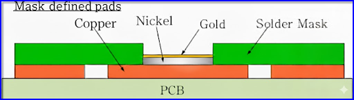
The contact pads within these areas can be fabricated using eithers solder mask-defined (SMD) or copper-defined (NSMD) pad designs. The following images illustrate both of these concepts:
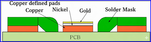
Copper Defined Pads (Non-Solder Mask Defined)
Copper-defined pads, also known as non-solder mask defined (NSMD) pads, feature copper pads that are smaller than the surrounding solder mask opening. This design provides better dimensional control and tighter tolerances, making it the preferred choice for most socket BGA designs where precise alignment between the socket contacts and the exposed copper surface is essential.
Solder Mask Defined pads
In solder mask-defined (SMD) pad designs, the copper pad is made larger, and the solder mask slightly overlaps the edges of the pad. This configuration provides stronger mechanical anchoring of the pad to the laminate, improving its resistance to mechanical stress. It is especially recommended for socket applications in high-stress environments where repeated insertions could otherwise cause the pads to lift or detach.
Which one to follow?
For BGA pitches of 0.65 mm or larger, non-solder mask defined (NSMD) pads are generally considered safe and reliable. However, for fine-pitch applications below 0.5 mm, solder mask defined (SMD) pads are sometimes required to prevent pad lifting that can occur due to increased contact pressure from the socket.
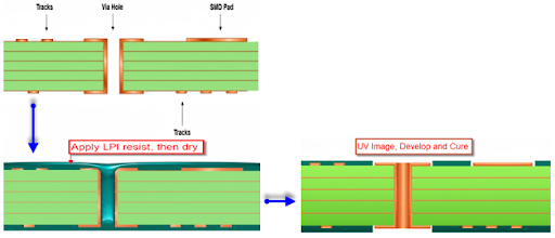
PCB Pad Height Requirement:
Most socketed BGA datasheets specify that the PCB pad height should be equal to or slightly higher than the surrounding solder mask. However, in practice, this condition is difficult to achieve. As shown in below figure, during manufacturing, the Liquid Photo Imageable (LPI) solder mask typically results in a coating that is higher than the PCB pad surface.
Surface Finish Requirements
The PCB surface finish plays a crucial role in socketed BGA applications, as the contacts are subjected to repeated friction and wear. Unlike permanent solder joints, socket interfaces require a finish that can resist oxidation, maintain consistently low contact resistance, and endure multiple insertion cycles. The following are common surface finish options suitable for such applications:
Hard Gold Plating (Electroplated)
The selection of a suitable surface finish depends primarily on the contact mechanism used in the BGA socket. Hard gold plating (electroplated) is excellent for mechanical durability, making it ideal for pogo-pin sockets that physically rub against the pad surface during repeated insertions. However, it is thicker, more rigid, and more expensive, and the electroplating process requires a bus bar plating method, which can complicate manufacturing. Moreover, since hard gold plating is not suitable for soldering, BGAs cannot be reflow soldered onto pads finished with hard gold, as the thick layer prevents proper solder wetting and can cause brittle solder joints, making it unsuitable for permanent BGA attachment.
Since hard gold plating is not compatible with soldering, BGAs cannot be reflow soldered onto pads with a hard gold finish. The thick, durable gold layer interferes with proper solder wetting and can lead to brittle joints, making it unsuitable for permanent soldered BGA assemblies.
In contrast, EPIG (Electro-less Palladium Immersion Gold) and EPAG (Electro-less Palladium Autocatalytic Gold) provide flat, uniform, and thin finishes with excellent electrical properties and low contact resistance, but they lack the mechanical robustness of hard gold. These finishes are better suited for conductive elastomer or GT elastomer sockets, where there is no sliding or scraping motion, only gentle compression contact. Additionally, PCBs with EPIG or EPAG finishes allow BGAs to be reflow soldered later if required, providing greater flexibility in assembly and rework.
Final Thoughts (From Design to Reliability)
At RUSH PCB Inc., we know what it takes to build reliable socketed BGA assemblies. The success of a socketed BGA mainly depends on three closely connected factors:
- Contact Mechanism
- Solder Mask pad design
- Surface Finish Choice
By carefully addressing these requirements, RUSH PCB Inc. can ensure low resistance, reliable, and long lasting socketed BGA assemblies, even under the stress of multiple insertions and demanding operating environments.


