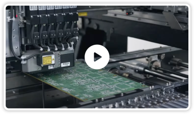
BGA Assembly Services
RUSH PCB is a California contract manufacturer specializing in complex BGA assembly services, including fine-pitch and micro-BGA assembly. Our rapid-turn prototype BGA PCB assembly services are available in as little as 24 hours from our Milpitas, California facility.
RUSH PCB is ISO 9001:2015 and ISO 13485:2016 certified. All of our BGA services are completed to the requirements of IPC-A-610 (Class 2 or 3) and J-STD-001.
Call us at 1-408-496-6013 for a quick-turnaround quote or fill out our online quote form.
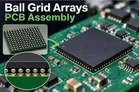
Preventing Ball Grid Array Assembly Defects
A Ball Grid Array (BGA) package is very unforgiving. All of the solder joints are hidden and therefore not accessible for direct visual inspection. An assembly mistake can happen without being discovered until the final product is tested. One small issue can ruin an assembly worth a thousand dollars or more.
BGA failures are associated with several root causes, many of which occur during controlled stages of the assembly process. Those causes and our process controls are listed below.
| Failure mode | Root cause | Control |
| HIP | Ball and paste do not coalesce | Reflow-profile control of paste volume and shape; X-ray verification |
| Popcorning/delamination | Moisture in the package body vaporizes into steam | Storage and floor-life control in accordance with J-STD-033; bake-out before reflow |
| Excessive voiding | Volatiles become trapped in the joint | Solder-paste selection in line with IPC-7095 guidelines |
| Opens/non-wets | Thermal gradient across the package | Delta-T control during reflow |
| Bridging/solder balling | Stencil-printing process is not adequately controlled | AOI and X-ray inspection |
BGA assembly processes can accommodate a wide variety of packages, including memory devices, large FPGAs, SoCs, and other high-ball-count packages. Automated placement of BGA components is facilitated by camera systems that control placement accuracy. Packages with 0.4 mm and 0.5 mm pitches are placed routinely; finer pitches are evaluated on a case-by-case basis.
We use hand placement for spacing from 0.025” to 0.070”, except for high-density interconnects (HDI), which can be as fine as 0.005” spacing. Blind or buried microvias with a diameter of 0.020” or less can be plated using laser drilling. We can also perform via fill.
All components are soldered using lead-free alloys unless specified otherwise. We can also provide standard SnPb alloys or develop a tailored alloy to meet your requirements. Solder-paste stencils are inspected before use. Alternatively, we can perform AOI to ensure 100% stencil coverage. X-ray inspection is also available to validate BGA assembly.
Our standard workmanship meets Class 2 or Class 3 of IPC-A-610. Class 3 workmanship can be specified for medical devices. Faster-turnaround requests receive priority. We also offer kitted and/or consigned services, as well as turnkey assembly.
BGA Rework Services
Our services include:
- Controlled hot-air or IR BGA rework
- Solder-residue removal
- Reballing
- BGA replacement and reflow
- Post-rework X-ray
- Failure analysis
These services can be especially useful when a component is obsolete or single-sourced and has a long lead time—for example, 40 weeks. In such cases, scrapping the board may not be an option. Learn more about our PCB assembly rework services.
Free DFM Review for BGA Designs
We also provide a free DFM review, with suggestions to help improve fanout design and BGA land patterns.
We have found that design issues surrounding the BGA can contribute to yield problems. Because RUSH PCB fabricates and assembles the circuit boards we review, we can assess the design and manufacturing considerations together in a single pass.
For each BGA quote, we evaluate:
- Choice of NSMD or SMD pads and pad-to-ball ratio
- Dog-bone fanout and via-in-pad
- Solder wicking and the need for via-in-pad plated over
- Feasibility of routing escape nets at 0.5 mm and 0.4 mm pitches, as well as general routability for very fine pitches
- Registration of solder mask and solder stencils
- Thermal stress and deformation of large copper planes
- Component clearance for rework and reflow
- Component courtyards
- Panelization and tooling
- Fiducials
- Stand-alone fiducial pads for individual BGAs (typically 4 fiducials) to ensure precise placement, fine-tuning, and streamlined rework, independent of overall PCBA fiducials
- Thermal balance
- Stackup and HDI microvias
- Escape routing
Because we also control bare-board fabrication, we can include controlled impedance, blind and buried microvias, and other advanced features. We can provide laser drilling of microvias and integrate the design and manufacturing requirements for BGA assembly in a single pass. See our HDI capabilities for more information.
Related capabilities: HDI Capabilities, Flex and Rigid-Flex Circuits, Printed Circuit Board Assembly, and PCB Assembly Rework Services.
Why Choose RUSH PCB for BGA Assembly?
- Fabrication and assembly of printed circuit boards in Milpitas, CA
- ISO, J-STD, IPC, UL, and RoHS certifications
- Military, aerospace, and safety-critical assembly
- High-speed prototyping and assembly
- Customers include Google, Nvidia, GE, NASA, Fitbit, and Sandia National Laboratories
“We have powered and programmed the first of the boards, and it is powering and programming and communicating with other boards via a number of small-pitch BGAs. You folks have done a fantastic job, and you have earned our business for all our safety-critical PCBAs.”
— Scott Hiatt, Sr. Engineer
Common Applications
- Aerospace avionics and radar/sonar
- Defense, medical and dental imaging, and other Class III devices
- Optical transport and other high-speed networking
- Data centers and other server and storage systems
- Automotive and other safety and collision-avoidance systems
- Industrial, communication, and control systems
- RF, microwave, and other systems
- Test and measurement systems and prototypes
BGA PCB Assembly Questions and Answers
What is BGA PCB assembly?
BGA PCB assembly is the process of attaching a Ball Grid Array (BGA) surface-mount device to a printed circuit board (PCB). First, solder paste is screen-printed onto the PCB in the area known as the land pattern. The BGA is then placed using a vision aligner and sent through an oven or reflow soldering machine to melt the solder paste and attach the package to the PCB.
Because the solder balls collapse onto the land pattern to form the joints, those joints are not directly visible. An X-ray machine is therefore used for final inspection.
What are the benefits of a BGA vs. a QFP?
A BGA takes less board space than a Quad-Flat Pack (QFP). A BGA can also allow for faster signal speeds because the interconnects and die are smaller and therefore have less inductance.
A BGA is a two-layer package. The first layer can be completely empty, while the second can be completely filled. This makes the package suitable for high-density interconnect (HDI) boards.
What is the smallest BGA pitch that RUSH PCB can assemble?
We routinely assemble 0.4 mm and 0.5 mm BGA pitches. We can also assemble CSP and PoP (Package on Package) devices. Smaller pitches are evaluated based on the design. To provide a quote, we need a complete set of design files, such as Gerber files, and your Bill of Materials (BOM). See our BGA capabilities for more information.
Do you perform X-ray inspections on all BGA assemblies?
We use X-ray inspection because BGA joints cannot be inspected with an AOI tool. X-ray can identify defects such as voids, opens, shorts, bridging, insufficient solder, and ball-to-ball interface defects. We evaluate these defects against applicable IPC standards, including IPC-7095 and IPC-A-610. X-ray inspection reports can be included in the build documentation upon request.
What is the maximum allowable number of voids in BGA solder joints?
The maximum allowable number of voids and the allowable area of each void depend on the product class and applicable requirements, including IPC-7095. Class 3 requirements are generally more restrictive than those for commercial Class 2 products. Void criteria are established for the product before production and documented.
Can you replace a BGA after PCB fabrication is completed?
Yes. We can remove and replace a BGA after it has been assembled on the PCB using hot-air or IR rework. Before performing the rework, we evaluate the PCB assembly for corner bonding or underfill around the BGA, since these can affect the process. The reworked BGA interconnects are evaluated using X-ray inspection.
Is underfill or corner bonding required for all BGA assemblies?
No. Underfill or corner bonding is normally used for products exposed to shock, vibration, or extreme thermal cycles—for example, handheld, automotive, or aerospace products. Underfill makes BGA rework extremely difficult, so it should only be used when required.
How do you assemble BGA packages?
We can assemble a range of BGA packages while controlling the moisture-sensitive period (MSP) based on each device’s sensitivity level. Moisture-sensitive devices are stored in dry packaging and dry cabinets. Components are baked before reflow soldering in accordance with J-STD-033.
Do you assemble flexible PCBs and HDI boards?
Yes. We assemble BGAs on flexible (Flex), rigid-flex, and HDI boards. We can fill blind and buried vias, perform via-in-pad and via fill, and support laser drilling, microvias, stacked vias, and other advanced interconnect technologies.
How long will it take to get a BGA prototype?
We can build prototype BGA assemblies quickly, with rapid-turn options available from our Milpitas facility. Turnaround depends on the project requirements. We can provide turnkey BGA assembly quotes based on your BOM.
Do you assemble BGAs to IPC Class 3?
Yes. We build to IPC-A-610 Class 3 and J-STD-001 requirements. RUSH PCB is ISO 9001:2015 and ISO 13485:2016 certified and provides military and aerospace assembly. Contact us to discuss your specific requirements.