As a leading provider of PCB prototyping, manufacturing, assembly & fabrication services in California, our mission at Rush PCB Inc. is to provide the best-in-class solutions for our customers. For this, we offer our engineering expertise and personalized services, thereby exceeding our clients’ expectations.
Our success in the industry is based on our responsiveness and unique service. Not only are we making a difference in the marketplace, but we are also building lasting relationships with our customers and suppliers based on our trust and integrity.
PCB Fabrication California
Our Technological Capabilities
- Metal Core PCBs — Aluminum
- LED PCBs
- Rigid PCBs
- Flexible PCBs
- Rigid-Flex PCBs
- High-Frequency PCBs
- HDI PCBs
- High-Tg Boards
- Thick Copper Boards
Advanced PCB Manufacturing Company in California
When our customers order advanced PCBs from Rush PCB Inc., they buy quality that pays for itself over time. Incidentally, PCBs show little differences even when they differ in inherent quality. That’s because the critical difference lies under the board’s surface, affecting its functionality and durability, and the difference is hidden from the customer. Nevertheless, they can rest assured that we push the envelope such that they, in turn, receive products that always meet the most stringent quality standards.
For us, no order is too small or too large. Whether it is large-scale PCB manufacturing in California or a few highly specialized precision PCBs, we always offer our customers the best possible time to market, so that they can maintain their competitive advantage. We offer our affordable PCB assembly in California at sustainable, low total costs because of our higher competence, proven delivery accuracy, and superior product quality.
PCB Assembly Services in California
We provide cutting-edge solutions through our personalized services and excellence in engineering. For instance, we provide low Dk and low Df materials and ELIC rigid-flex boards. We use semi-additive processes to offer 35 µm lines and spaces. In fact, we have designed our entire range of printed circuit boards to fit all our customers’ needs.
As a professional quick-turn PCB manufacturer in California, we offer PCB prototyping, PCB assembly, and large-scale production manufacturing in the US. Our quick-turn offer is for small-quantity production, custom specifications, standard PCBs, and quick-order PCBs.
Listed below are our advanced capabilities for quick-turn PCBs:
| Items | Manufacturing Capabilities | Remarks |
| Number of Layers | 1-10 layers | For orders above 10 layers, please contact our sales rep. |
| Material | FR-4, Aluminum | For Rigid, Rigid-flex, Flex, Metal-based (Aluminum etc.), Halogen-free, HDI, High Tg, etc., please contact our sales rep. |
| Maximum PCB Size | 500 x 1100 mm (min 5 x 6 mm) |
Any sizes beyond this dimension, please contact our sales rep. |
| Board Size Tolerance (Outline) | ±0.2 mm / ±0.5 mm | ±0.2 mm for CNC routing, and ±0.5mm for V-scoring. |
| Board Thickness | 0.2 to 2.4 mm, with 0.2 mm increment. | If your board exceeds these, please contact us. |
| Tolerance of Board Thickness (t ≥ 1.0mm) |
±10 % | “+ Tolerance” typically occurs due to PCB processes like electroless copper plating, solder mask, and other types of surface finish. |
| Tolerance of Board Thickness (t < 1.0mm) |
±0.1 mm | “+ Tolerance” typically occurs due to PCB processes like electroless copper plating, solder mask, and other types of surface finish. |
| Min Trace | 0.1 mm / 4 mil | Min trace we can fabricate is 4 mils (0.1 mm). We strongly suggest designing traces above 6 mils (0.15 mm) to lower costs. |
| Min Spacing | 0.1 mm / 4 mil | The min spacing we can fabricate is 4 mils (0.1 mm). We strongly suggest designing spacing above 6 mils (0.15 mm) to lower costs. |
| Outer Layer Copper Thickness | 1 oz / 2 oz / 3 oz (35 μm / 70 μm / 105 μm) |
Also known as copper weight. 35 μm = 1 oz, 70 μm = 2 oz, 105 μm = 3 oz. Contact us if you need copper weight greater than 3 oz. |
| Inner Layer Copper Thickness | 1 oz / 1.5 oz (35 μm / 50 μm) |
For 4 and 6 layers (Multi-layer laminated structure), the inner copper weight is as per the customer’s request. Please contact us if your required copper weight is greater than 1.5 oz. |
| Drill Sizes (CNC) | 0.2-6.3 mm | Min drill size is 0.2mm, max drill is 6.3mm. Any holes greater than 6.3mm or smaller than 0.3mm will attract extra charges. |
| Min Width of Annular Ring | 0.15 mm (6 mil) | For pads with vias in the middle, Min width for Annular Ring is 0.15 mm (6 mil). |
| Finished Hole Diameter (CNC) | 0.2 mm-6.2 mm | The finished hole diameter will be smaller than the size of the drill bit because of copper plating in the hole barrel. |
| Finished Hole Size Tolerance(CNC) | ±0.08 mm | For example, if the drill size is 0.6 mm, the finished hole diameters ranging from 0.52 mm to 0.68 mm are acceptable. |
| Solder Mask | LPI | Liquid Photo-Imageable is the most popular. We use thermosetting Ink in inexpensive paper-based boards. |
| Legend Minimum Character Width | 0.15 mm | Characters of less than 0.15 mm wide are too narrow to be identifiable. |
| Legend Minimum Character Height | 0.8 mm | Characters of less than 0.8 mm high are too small to be recognizable. |
| Legend, ratio of Character Width to Height | 1:5 | This is the most suitable ratio for PCB silkscreen legends processing |
| Minimum Dia. of Plated Half Holes | 0.6 mm | Design all Half-Holes to be larger than 0.6 mm. This ensures better connection from board to board. |
| Surface Finishes | HASL with lead, HASL lead-free, OSP, Immersion gold | The most popular three types of PCB surface finish. Please contact us for other finishes. |
| Solder Mask | Yellow, Green, Red, Blue, Black, White | No extra charge for Green, Red, Yellow, and Blue solder mask |
| Silkscreen | Black, White, None | No extra charge for silkscreen. |
| Panelization | Tab-routing, perforation holes (Stamp Holes), and V-scoring | Leave a minimum clearance of 1.6 mm between boards for break-routing. For V-score panelization, set the space between boards to be zero. |
| Others | Fly Probe Testing (Free) and A.O.I. testing (free), ISO 9001:2015, IATF 16949, UL Certificate | No extra charge. |
We also offer advanced services, including full-spec PCBs, highly specialized precision PCBs, and large-scale production quantities. For fast turnarounds, we have a dedicated customer service team, and we ensure that we exceed our customers’ expectations.
Experts in PCB Fabrication and Assembly in California
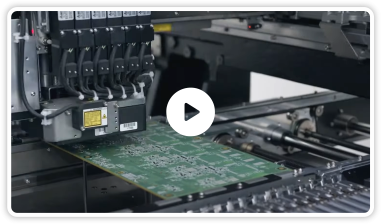
Our California turnkey PCB assembly process is for mounting and soldering electronic components onto printed circuit boards. We offer our California PCB assembly solutions with the fastest delivery times. We use surface mount, through-hole, and mixed technology components to assemble printed circuit boards as per our customer requirements. Our high-quality PCB assembly California ranges from prototypes to large production orders.
As a leader in rendering incomparable PCB manufacturing and assembly services, we ultimately deliver high-end technology to our customers. Whether their requirements are for quick-turn PCB manufacturing California or large-scale PCB production California, we offer our renowned craftsmanship. We offer our customers a broad product mix that includes features such as blind, buried, and micro-vias.
Why Rush PCB Inc.?
As a highly reliable and reputed PCB assembly company located in California, USA, Rush PCB Inc. serves clients all over the country. With more than two decades in the field of PCB prototyping and fabrication, we aim to meet the needs of our customers across industries with unequaled quality, delivery, cost-effectiveness, and other demanding requirements. As one of the highly experienced PCB manufacturing experts in California, US, we pride ourselves in being the best business partner for our customers and a good friend in need for any aspect of PCBs. Our exceptional qualities:
- Best value manufacturer with direct pricing
- Fast turnarounds — as fast as 24 hours
- No minimum quantity requirements
- On-time shipping delivery rates 99%
- 300+ active world-class customers across the globe
Quick-Turn PCB Assembly, Prototype, and Fabrication
If you are looking for highly reliable, high-quality manufacturing and PCB assembly services in California, you have come to the right place. Rush PCB Inc. provides quick-turn PCB design, prototyping, fabrication, and assembly to industries in California and surrounding areas.
With upwards of two decades of PCB fabrication and assembly services of various complex configurations, we are confident of meeting all your application requirements.
In case you are looking to source PCB assembly in California, we will serve you better. We have the capabilities that we have acquired over the years and which allow us to meet all customer requirements above their satisfaction. We offer:
- SMT and Through-Hole Assembly
- Reflow Soldering for PCBA
- Wave Soldering for PCBA
- Flex and Rigid-Flex PCB Manufacturing
- Rigid, HDI, and ELIC (Any Layer) Board Manufacturing
- One-Stop BOM Purchase Solutions
- Box-Build Manufacturing Solutions