


This article presented by RUSH PCB Inc., provides a complete overview of ELIC technology, beginning with its stack-up architecture and manufacturing process flow, and moving into the critical challenges of copper plating, planarization, and microvia reliability. We also explore IPC standards and compliance requirements, along with key design for manufacturing and CAM considerations that determine successful production. We shall examine both the manufacturing challenges and cost implications involved.
Finally, we look ahead to emerging trends that will shape the future of ELIC PCB manufacturing and enable the next generation of compact, high-speed electronic systems.
Overview of ELIC Technology
At its core, ELIC technology eliminates the use of mechanically drilled through vias and buried vias entirely. Instead, each conductive layer is interconnected using microvias formed by laser drilling and copper plating. Unlike conventional sequential HDI structures such as 1+N+1 or 2+N+2, where microvias are limited to outer buildup layers, ELIC allows microvias to exist between every adjacent layer.
This architecture significantly shortens signal paths, reduces parasitic inductance, and enables very compact routing, making it ideal for advanced electronics where space and performance are critical. However, these benefits come at the cost of increased manufacturing complexity, tighter process control, and higher fabrication costs.
ELIC Stack-Up Architecture in Rigid PCBs
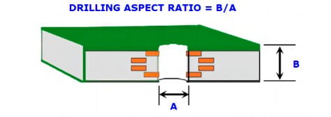
ELIC rigid PCBs use very thin dielectric layers optimized for laser drilling and sequential lamination, making stack-up planning critical to success. Prepregs with a preferred resin content of 65–75% are commonly selected to ensure clean laser ablation, stable microvia walls, and good thermal reliability. Laser drilled microvias are typically designed with a safe aspect ratio of 0.8:1 to 1:1 to support reliable copper filling and long-term performance.
To enable fine-line imaging and consistent planarization, ELIC stack-ups usually start with thin base copper foils of 1/4 oz to 1/3 oz, maintaining stack-up symmetry, as multiple lamination cycles and thin dielectrics can otherwise lead to warpage. Early stack-up validation with the fabrication and CAM teams remains one of the most important steps in any ELIC design.
Manufacturing Process Flow of ELIC Rigid PCBs
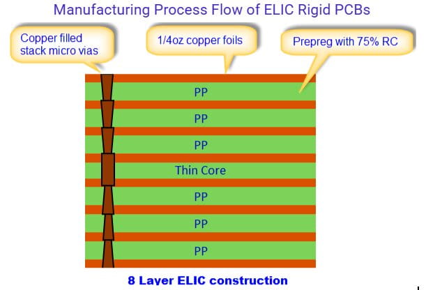
The manufacturing process of ELIC rigid PCBs use a step by step buildup method, similar to HDI boards but with more repeated steps and tighter control. It starts with making a very thin core layer. This core is laser drilled to create microvias, which are then plated and copper filled. After that, the copper patterns are formed using imaging and etching.
Next, this finished core is laminated between two thin copper foils using resin rich prepreg sheets. The same steps i-e laser drilling, copper filling, imaging, and etching of the copper layers are repeated to add the next set of layers. This buildup continues until all layers are completed. Throughout the process, microvias must be extremely accurate in size, depth, and alignment, since even small errors can cause reliability issues.
Microvia Structures, Copper Plating, and Reliability Considerations
When designing ELIC PCBs, microvia quality is the key to overall reliability. In most ELIC structures, microvias are stacked rather than staggered to maximize routing density. This improves performance and compactness but places higher demands on copper integrity and plating quality.
Typical laser drilled microvias have diameters of 75–100 µm (3–4 mil) and depths of 60–80 µm, keeping the aspect ratio between 0.8:1 and 1:1 to ensure reliable copper filling. Plating thickness at the via knee is usually 20–25 µm to withstand thermal cycling.
Exceeding these limits by making vias too deep, narrow, or misaligned can cause via cracking, copper separation, or barrel fatigue, especially under repeated thermal stress. To prevent these issues, we often have to enforce stricter internal rules than IPC minimums.
For reliability, IPC Class 2 supports standard commercial applications, while IPC Class 3 (defined in IPC-6012 for rigid PCBs and IPC-6016 for HDI/microvias) requires tighter control over microvia integrity, plating uniformity, and registration. Consistent dielectric thickness, resin control, thin base copper, and balanced copper layouts all help meet these higher standards.
IPC Standards and Compliance Requirements
Industry standards provide an important guide for ELIC PCB manufacturing, even as the technology evolves. IPC-2226 recommends laser drilled microvia diameters of 75–150 µm (3–6 mil), via depths of 60–100 µm, and aspect ratios between 0.8:1 and 1:1 for stacked and staggered microvias, along with proper stacking and lamination practices to reduce stress and warpage.
IPC-6012 and its HDI supplement documentation define performance and reliability requirements, including minimum copper plating thickness of 20 µm in microvias, and lamination quality standards to ensure long term electrical and mechanical integrity.
IPC-A-600 sets visual inspection criteria, such as allowable microvia voids (<5%), acceptable surface finishes, and copper fill quality to determine if a board is acceptable. In practice, fabrication shops often apply more conservative limits based on their equipment and yield history. CAM engineers must therefore understand both the official IPC values and the practical capabilities of the chosen fab to produce reliable, manufacturable ELIC designs.
Design for Manufacturing and CAM Considerations
DFM considerations are especially critical in ELIC projects. Fine trace widths and spacing must be matched to the PCB vendor’s imaging capability, and microvia pad sizes must provide sufficient capture area without wasting routing space. VIPPO designs are common in ELIC boards, but they require fully filled and planarized vias to avoid soldering defects like solder bridging and via failures during PCB assembly.
From a CAM perspective, ELIC designs demand thorough checks for stack-up consistency, microvia alignment, annular ring adequacy, and copper balance. Any ambiguity in design data can quickly translate into manufacturing risk, so clear fab notes and early technical alignment are essential.
Manufacturing Challenges and Cost Implications
Despite its advantages, ELIC technology presents several challenges that must be carefully managed. Fabrication is more complex due to thin dielectric layers, stacked microvias, tight aspect ratios, and precise copper plating requirements, which demand advanced equipment and strict process control. Costs are significantly higher than conventional multilayer or standard HDI boards because of multiple lamination cycles and yield sensitivity.
Lead times can also be longer, especially when stack-up changes or design iterations are needed. Repair and rework are particularly difficult, as defects in stacked microvias, thin dielectric layers, or copper fills are often inaccessible once the board is laminated, making it almost impossible to correct internal failures. This makes first-pass success critical. These factors highlight the importance of early collaboration between design, CAM, and fabrication teams to reduce risk and ensure reliable production.
Future Trends in ELIC PCB Manufacturing
Looking ahead, ELIC technology will keep advancing as the need for more connections in smaller spaces grows. We can expect smaller microvias, more layers, and better materials that handle higher speeds and heat more effectively. The line between advanced PCBs and IC packaging is also blurring, with ELIC acting as a bridge between traditional boards and semiconductor technologies. As fabrication processes improve and capabilities grow, ELIC will become easier to produce, while still remaining a premium choice for high-performance applications
ELIC PCB Innovation Made Simple with Rush PCB
ELIC PCB designs can be tricky, with thin layers, stacked microvias, tight aspect ratios, and precise copper plating requiring careful control. At Rush PCB, we make it easy. Our expert engineers guide every step from design and CAM to fabrication ensuring first pass success and minimal risk. With deep know how in materials, lamination, and plating technologies, we keep costs down, yields high, and lead times on track. For high density, high performance PCBs, Rush PCB makes even the most advanced ELIC designs feel effortless.


