


LGA Packaging 101: A Guide to Design, Assembly, and Inspection
What Exactly Is LGA?
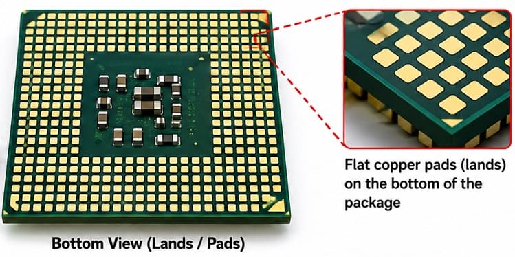
Land Grid Array or LGA, is one of the types of surface mount packaging technology that we normally use for ICs, processors, sensors etc. LGAs don’t have pins or solder balls sticking out, instead they have a flat grid of metallic pads on its underside to mate with matching pads on the PCB.
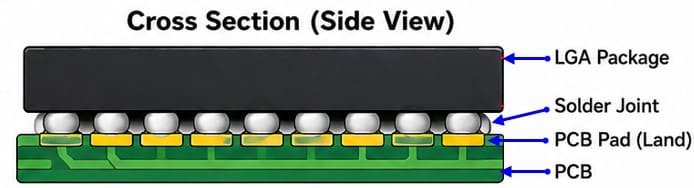
As an example, Intel Core i7/i9 and AMD Ryzen desktop processors both use LGA sockets. Whenever high pin density, compact size, and good thermal behavior matter, LGA packaging is the solution. Interestingly, while soldering LGAs on PCBs, we have pads on both ends but the solder paste is always sitting on the pads on the PCB. We should always remember it.
Where Is LGA Used?
Land Grid Array (LGA) style of packaging is normally deployed where we have high-performance and space-limited electronic systems. We use it for desktop processors, server CPUs, embedded systems, and advanced computing devices. Since we don’t have pins or balls on the LGA package, we connect the chip directly to the PCB through a flat pad-to-pad contact structure using solder.
This direct connection not only allows a higher number of connections in a smaller space but also reduces unwanted electrical effects like parasitic inductance which helps improve signal quality. These benefits make LGA one of the most suitable candidate to be widely used in processors and systems where performance and efficiency are critical.
The Good and the Not-So-Good
Strengths
-
Better heat dissipation: Since heat sinks are attached to the chip surface directly, it helps keep the temperature lower.
-
Stronger electrical performance: Shorter, denser interconnects result in less noise and faster signals.
-
No bent pins: Handling and installation damages reduce significantly due to the absence of protruding pins.
-
Higher connection density: Smaller pads packed at tighter means higher I/O density in a smaller footprint.
Drawbacks
-
Soldering is tricky: As joints are hidden under the package. We can only inspect those using X-rays.
-
Surface flatness is critical: Concerns related to board warpage are higher as it can result in poor contact.
-
Short-circuit risk: Tight spacing increases the possibility of creating short due to bridging during assembly.
-
Higher process cost: Smaller tolerances require more precise equipment and stricter quality control.
Notable Characteristics of LGA
With LGA packages, we get higher number of electrical connections within a small area. This helps designers create denser and space-efficient PCB layouts.
Low Profile
Due to the absence of protruding pins, the package sits very close to the PCB surface. This makes LGA suitable candidate to be part of slim and lightweight electronic devices.
Good Thermal Path
In LGA packages, the heatsinks are closer to the active area hence heat transfer from the semiconductor die to the PCB or heatsink is very effective. This improves thermal management and overall device reliability.
No Insertion Force
The absence of the protruding pins, the LGA packages sits flat on the PCB without requiring any mechanical insertion. This reduces stress on both the component and the board during assembly.
SMT Friendly
LGA components are highly compatible for automated surface-mount assembly processes. Pick-and-place machines can pick them up and place them with higher accuracy and precision.
Low Signal Delay
Since there are no pins, hence the values of parasitic capacitance and inductance reduce drastically. It improves signal integrity and high-speed electrical performance.
Reliable Contact
The flat pad-to-pad connection design provides stable and consistent electrical contact. Tight manufacturing tolerances also help reduce assembly defects.
Better Security
The close-contact adds an extra level of protection against unauthorized access or tampering.
How LGA Packages Are Made
The manufacturing flow for an LGA package follows these steps:
1. Die Preparation
Silicon wafer is diced to achieve individual semiconductor chips. and prepared for packaging. The individual dies are prepared for packaging using encapsulation material to prevent physical and environmental damage.
2. Solder Deposition
The chip is placed onto the substrate in a face-down orientation. For accurate electrical connections, we use stencil printing to apply the solder paste on the connection pads.
3. Reflow Soldering
The assembled package is then passed through a controlled heating chamber. During reflow, the solder melts and forms strong electrical and mechanical bonds between the die and substrate.
4. Cleaning
Once the soldering process is complete, contaminants and flux residues are removed from the package surface. It helps improve reliability and prevents corrosion or electrical issues.
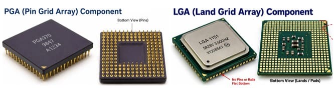
LGA vs PGA: What’s the Difference?
In PGA, the chip has pins, which insert into holes in a socket on the motherboard. It is simple but those pins bend easily.
In LGA, the chip has flat pads and the socket on the motherboard has spring contacts. So there is no concern of pins to bend which makes LGA more robust during installation. The trade-off is that LGA sockets are more expensive to manufacture. In short:
-
PGA = pins on the chip.
-
LGA = pads on the chip, contacts on the socket.
-
LGA wins on durability; PGA wins on simplicity.
Soldering LGA: Step by Step
1. Clean the PCB Pads
The PCB pads are cleaned to remove oxidation, dust, or contaminants that may affect soldering quality. Flux is then applied to improve solder wetting and ensure proper joint formation.
2. Apply Solder Paste
Solder paste is deposited onto the PCB pads using a stencil printing process. The stencils are designed to ensure correct paste volume to avoid insufficient solder or bridging defects.
3. Place the Component
The Land Grid Array (LGA) component is carefully aligned so its lands match the PCB pads accurately. Proper placement is critical because LGA packages do not have visible leads for alignment support.
4. Reflow
The assembled PCB passes through a reflow oven with a controlled temperature profile. During heating, the solder paste melts and creates reliable electrical and mechanical connections.
5. Cool Down
After reflow, the board is cooled naturally to allow the solder joints solidify properly. Rapid cooling may introduce stress or weaken the solder joints.
6. Inspect Joints
Since the solder joints are hidden so we adopt visual method or X-ray inspection to verify the quality of joints. This step is done to identify defects such as opens, bridging, voids, or misalignment.
7. Clean Again
Remove the flux residue or contaminants from the PCB surface using isopropyl alcohol or suitable cleaning agents. Proper cleaning is important for long-term reliability and prevention of corrosion.
8. Test
The assembled board is then powered up to verify proper electrical operation. Functional testing is carried out to confirm the proper working of the LGA component and surrounding circuitry.
Common Soldering Issues and How to Fix Them
Insufficient Solder
Not enough paste on the pad leads to a weak or open joint. Fix it by reviewing your stencil apertures and paste volume.
Bridging
Excess solder flows between adjacent pads and creates short circuits. Use smaller stencil apertures and check your paste deposit consistency.
Head-on-Pillow (HOP)
The component sits at an angle because one pad did not reflow properly. Slow down the ramp rate or extend the soak phase in your reflow profile.
Pitting
Small holes appear on solder balls or joints from excessive heat or outgassing. Using OSP surface finish and controlling peak temperature usually resolves this.
Non-Wet Open (NWO)
Solder does not properly spread and stick to the pad after cooling. This issue is usually caused by trapped gases and increasing the preheat temperature often helps fix it by reducing outgassing.
Design & Build Considerations
At RUSH PCB Inc, we leverage our expertise in PCB manufacturing and assembly to help clients optimize LGA layouts for thermal and signal integrity.
PCB Layout
LGA packages always have high speed interface login in them so signal and power traces must be planned carefully to minimize noise, interference, and crosstalk. These packages have high pin density at smaller pitches so sufficient space and clearance should be provided around the Land Grid Array (LGA) package for proper routing and assembly reliability.
Thermal Management
Due to high speed and dense logic packed in LGA packages, they generate significant heat during operation. We should deploy heatsinks, thermal vias, or dedicated thermal pads in the design dissipate the heat generated and maintain safe operating temperatures.
Reflow Profile
During reflow soldering process, higher temperature build ups can damage the package, PCB, or solder joints, while insufficient heating may result in poor solder connections. So attention must be paid to designing and controlling the reflow soldering temperature profile during the assembly.
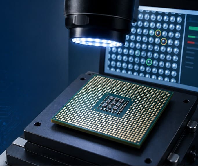
Inspection
Since the solder joints of LGA packages are hidden underneath the component, inspection is extremely important after assembly. Techniques such as X-ray inspection are commonly used to detect defects like opens, bridging, or voids.
Ways to Inspect an LGA Assembly
Visual Inspection
This inspection method focuses only on visible quality checks such as exposed edges, pad alignment, cleanliness, and any obvious surface defects on the assembly. It is quick, simple, and cost-effective, but we cannot see hidden solder joints under the Land Grid Array (LGA) package.
X-Ray Inspection
X-ray inspection is the most critical method for checking Land Grid Array (LGA) assemblies. It allows you to see through the package body and clearly identify hidden defects such as voids, solder bridges, opens, and uneven solder distribution. For any quality-critical product, this step is essentially non-negotiable to ensure reliable solder joint formation and long-term performance.
Automated Optical Inspection (AOI)
AOI is very effective, but we use this method before the reflow process starts. It helps us detecting placement errors and visible surface defects. However, we use X-ray inspection view the hidden solder joints of Land Grid Array (LGA) packages. So AOI is always used in combination with X-ray inspection rather than as a replacement.
Electrical Testing
Apply signals to the circuit and measure its response to detect functional issues such as opens or shorts that impact performance. While this helps confirm overall electrical operation, it works best as a complement to X-ray inspection, since it cannot reliably reveal the condition of a weak or marginal joint that still happens to pass electrical testing.
Environmental Testing
In order to uncover long-term reliability issues that may not appear during initial inspection or functional testing, we carry out thermal cycling, vibration, and humidity testing. These tests are very important for electronic products that are designed to function in harsh environmental conditions, where mechanical and thermal stresses can de-grade solder joint integrity and overall performance.
Summary
Land Grid Array (LGA) is a well-established and high-performance packaging technology that offers advantages in I/O density, electrical performance, and thermal management. It is especially useful in applications where higher connections densities are required within limited PCB space or where signal integrity and heat dissipation are critical. Although LGA assembly comes with certain challenges such as precise soldering requirements, hidden joint inspection through X-ray analysis, and difficult rework procedures, these issues can be effectively managed with proper PCB footprint design, a controlled reflow soldering process, and reliable inspection methods. When handled correctly by experienced manufacturing partners like RUSH PCB Inc, LGA packages provide highly consistent and dependable performance in modern electronic systems.


