

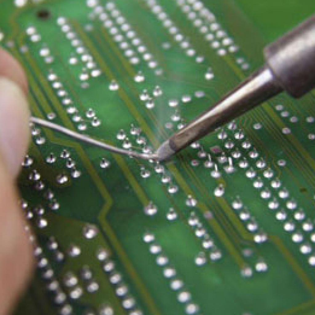
Most of the solder the electronic industry uses today is of the lead-free variety, as use of lead has been recognized as a health hazard. Lead-free solder melts at a higher temperature, and has introduced a variety of challenges. Rush PCB has compiled a list of solder defects that can help managers, designers, engineers, and operatives recognize these everyday problems and allow them troubleshoot efficiently and effectively.
The electronic industry uses the standard IPC 610D for the Acceptability of Electronic Assemblies. The standard offers criteria for lead-free soldering and has examples of typical process faults. The document is continually updated and will include more examples of lead-free soldering in the future.
According to Rush PCB, simply looking at a solder joint may not reveal the most common assembly and soldering defects associated with lead-free technology. This is because certain markets may not consider them as defects but variations in the process. However, only a thorough investigation can confirm the possible impact on the reliability or acceptability of the joint.
Common Lead-Free Solder Joint Defects
- Open joints
- Incomplete solder coverage
- Solderability failure
- Floating LGA
- Component Damage
- Solder skip
- Solder balls
- Fillet lifting in through holes
- Non-Coalescence of paste
- Popcorning/cracking
- Surface corrosion and copper dendrites
- Tin whiskers
- Incomplete reflow of pin in hole
- Insulation contamination
- Pad lifting
- Non-reflow of paste
- PCB Delamination
- Incomplete Wetting
- Solder Wicking
- Outgassing and Blowholes
Open Joints
This is the most common type of defect especially found under POP packages, where two or more Chip Scale Packages (CSP) or Ball Grid Array (BGA) components are placed one on top of the other and reflow soldered. Package warping is one of the main reasons for such open solder connections, which can cause one or multiple open connections.
Poor solderability may be another reason for the formation of open joints. Paste deposit extending too far under the body of the component may be another reason. The excess solder can lift the component and its lead above the surface of the solder paste as it reflows before allowing the lead to wet, leaving the joint open.
Incomplete Solder Coverage
Also Read: Preventing Corrosion in Printed Circuit Boards
Increased temperatures in lead-free processes can cause solder to solidify prematurely as the inner layers lose heat. This results in solder joints with a reduced hole filling.
Solderability Failure
This failure is more prominent in Land Grid Array (LGA) and Quad Flat No Lead (QFN) packages, as they often do not have solderable side terminations or the component manufacturing process has made them poorly solderable. Often, a lack of protective coating of tin on the surface of copper lead frame is the cause of poor solderability of the edge termination. Although IPC 610 does not require side terminations to be solderable, customers prefer to see a joint. Additionally, the presence of solder on the edge termination helps Automatic Optical Inspection.
Floating LGA
During reflow, Land Grid Array (LGA) packages may lift, resulting in open solder joints. This is mostly caused by excess solder paste under the center pad of the package causing the part to float on the surface of molten solder. This is easily corrected by changing the stencil design. The aperture for the center pad should be only 50-60% of the area of the pad. If possible, splitting up the area of the pad with 4-9 equally spaced apertures also helps.
Component Damage
Passing through the solder reflow process can be a tough time for Moisture Sensitive Devices (MSD), unless they are packaged properly to prevent them from mechanical damage from handling or cracking. Exposing such MSDs to high levels of humidity may lead to cracking of the component body or pop corning during reflow.
Solder Skip
This is a common defect in wave soldering caused by incorrect wave height. Usually, there is no solder on the pad or on the termination. However, process issues such as flux gassing should also be investigated along with wave height.
Solder Balls
This is a typical result of using paste to rework parts such as BGA, where excessive paste turned into a ball during reflow. The presence of the ball reduces the insulation separation distance below the required minimum. Solder balls can be removed with a high-pressure airline directed with care, but require a follow-up inspection with optical or x-ray.
Fillet Lifting in Through Holes
Lead-free soldering often causes fillet lifting in through-hole component leads. Sometimes, along with the fillet, the pad may be separated from the laminate as well. However, in most cases, this failure does not lead to a joint failure or an electrical failure. The main reason for this type of failure is related to the expansion and contraction the PCB undergoes during soldering and the solidification of lead-free materials. IPC 610D inspection criteria covers this process issue.
Non-Coalescence of Paste
With component sizes shrinking, small paste deposits often do not fully reflow in air, and this is very common with lead-free solder paste when operators use a traditional soak profile. The solder paste turns into balls that do not fully reflow into the bulk of the solder joint. This defect is common in 0201 and 01005 chip components during convection reflow. As the small deposit of solder paste is exposed for a long period of elevated temperature during the lead-free profile, it reduces the performance of the flux in the paste. The inert atmosphere in vapor-phase soldering does not allow this to happen.
Popcorning/Cracking of Components
Incorrect specification or use of the component can lead to its popcorning or cracking during the elevated temperature of lead-free solder reflow. This can be corroborated with the maximum soldering temperature and duration suggested by the manufacturer of the component.
Surface Corrosion and Copper Dendrites
Apart from flux, surface cleanliness on the PCB can lead to surface corrosion. Surface insulation resistance assessment and contamination testing are two common techniques for monitoring and controlling levels of harmful contaminants on the PCB surface to avoid corrosion.
Formation of copper dendrites can lead to intermittent failures in PCBs. Such failures are more common in lead-free soldering with VOC free fluxes. The culprit is the flux residue remaining on the board surface, which forms a conductive path through the moisture layer when the board is subject to high temperature and humidity.
Tin Whiskers
Tin coating on the surface of a PTH PCB can often lead to growth of tin whiskers that short neighboring tracks and pads. Tin is often the finish of choice in the electronic industry using lead-free soldering, but whisker formation is a concern. The whiskers mainly occur due to stress formed during the plating process.
Incomplete Reflow of Pin in Hole
Forming TH connector joints by intrusive reflow soldering offers a poor visual appearance after the soldering. The main cause is many of the paste particles not completely reflowing and coalescing into the joint. The culprit may be a long delay in the soak period of reflow before the PCB reaches reflow temperature, thereby exhausting the protective layer provided by the paste.
Insulation Contamination
This is a common fault in a wave soldering process when soldering insulated leads directly onto a circuit board, and the insulation is of a low temperature material. Pieces of insulation falling into the joint during the soldering process can contaminate the joint.
Pad Lifting
The higher temperature profile of the lead-free soldering process can cause the printed board material to expand in the Z-axis, thereby deforming or placing strain on the pad. This may result in the pad lifting off the surface of the PCB or the fillet lifting from the pad. The fillet may also tear in the process. The expansion and contraction of the laminate and the solder are the chief reason for pad lifting.
Non-Reflow of Paste
Non-reflow or incomplete reflow of solder paste is mainly caused by low profile temperature, resulting in non-wetting of the pad or component lead. Such non-reflow can happen when the component termination on the board fails to reach or remain at reflow temperature for the required time. The reason may be a wide difference in temperature across the board. Although it takes only a few seconds to form a reliable joint, the components forming the joint do have to remain at temperature above liquidus for a period of 40-60 seconds.
PCB Delamination
Delamination or an air gap, or blister is formed when water vapor from the PCB material expands and escapes during heating. The higher temperatures of lead-free places more energy on the materials, and delamination of the PCB materials may occur when moisture in the board expands during the reflow process.
Incomplete Wetting
Incomplete wetting is a result of reduced wetting characteristics of most lead-free alloys and the introduction of alternative surface finishes. Solderability of a printed board surface decreases in the order of finish, beginning with solder, gold, silver, tin, copper, and OSP. Depending on the surface finish present on a board, the lead-free solder paste may reflow to cover the pad totally or partially.
Solder Wicking
Solder wicking is a problem where the solder paste, during reflow, tends to wet the terminations of the component rather than the pad and the lead. Faster wetting of the termination and slow wetting of the pad could be due to problems with pad solderability., caused by a poorly cleaned board.
Outgassing and Blowholes
Moisture in the printed board may expand during the soldering process and outgas from the plated through holes. The gas comes out of the hole as water vapor when the solder is still in the liquid state. As the solder on the top side solidifies first, voids may be visible on the base of the board. The escaping gas causes pinholes, blowholes, or voids, with size related to the volume of the escaping gas.
Conclusion
Although the above compilation of solder joint defects by Rush PCB is in no way complete, they represent the most common problems faced by the industry. While some of the above problems are not related directly to the solder joint or its quality, they are a result of the higher process temperatures encountered during reflow because of the use of lead-free solder.


