How does Conductor Surface Roughness matter?
In RF circuit design, it is necessary to select the proper Printed Circuit Board (PCB) material for the application. In this context, modern simulation tools such as Computer Aided Engineering (CAE) help engineers by predicting the electrical behavior that circuits exhibit on various types of PCB materials. The tools use material parameters in their calculations, with dielectric constant (relative) being one of the important parameters. However, most such tools overlook an equally important material parameter of PCBs during the process of design—the roughness of the conductor’s surface. Contrary to popular belief, conductor surface is never perfectly smooth, and this has consequences in high-frequency PCB design.
Eminent PCB manufacturers such as Rush PCB Inc. understand the influence an imperfect conductor surface has on the performance of a PCB. In fact, scientists have since long studied the effect of grooves present on the conductor’s surface on a PCB, having noted the increase in losses caused by the grooves. Under worst-case scenarios, the grooves caused losses that were twice the original. The explanation the researchers extended was electromagnetic (EM) waves travel mostly along the conductor’s surface, such as along the copper signal trace on a PCB. The grooves actually cause the signal paths to become longer, as the EM waves, while traveling along the surface, have to enter into, and then exit out of the grooves.
Skin Effect
The surface roughness of the conductor thereby causes the EM waves taking a path with a longer mean resulting in the increase in losses. Effectively, higher the degree of surface roughness of the conductor, higher is the resistance from skin effects. When an EM wave propagates in a conductor, skin effect tends to change the EM wave’s current distribution to accumulate more towards the conductor’s surface rather than remaining deep inside the conductive material.
When using EM simulators or other commercial CAE tools, designers overcome the surface roughness of a conductor by relying on the traditional Morgan Correlation. They do this by involving a numerical factor for correcting the surface roughness, depending on the ratio of a smooth surface to a rough one. While calculating the loss of high-frequency microstrip lines, using Kr mostly does a good job of matching closely the results of measurement of conductor losses. However, there are cases where the measurements fail to match the computer predictions so closely.
Furthermore, such deviations between the calculated and the measured values can be expensive at the design stage, especially as achieving the desired performance requirements can lead to additional design iterations. Avoiding such delays in design might mean considering carefully the choice of an RF PCB laminate based on its conductor’s surface roughness.
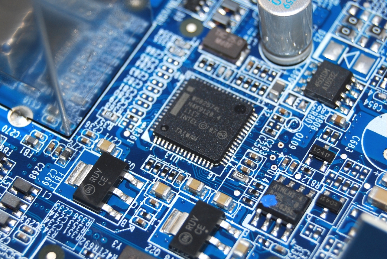
Types of Copper Cladding
Manufacturers have to use some form of a cladding of copper conductor on the PCB substrate. Three types are most common—electrodeposited (ED) copper, rolled-annealed (RA) copper, and reverse-treated (RT) copper.
Forming RA copper foils involves rolling the copper ingot through a rolling mill, where subsequent passes through the rollers of the mill results in a copper foil consistently thin.
ED copper formation requires depositing copper onto a slowly rotating, highly polished drum made of stainless steel, within a bath containing a solution of copper sulfate. While the roughness of the copper surface where it meets the stainless-steel drum is analogous to that of RA copper, the copper surface of the deposition side facing the solution is much rougher.
RT foil production starts by plating the ED copper foil on the drum side, when the foil on the bath side is still low profile.
As the copper foil has to adhere to the dielectric material, which may range from FR-4 to polytetrafluoroethylene (PTFE) substrates, the copper surface has to be treated to increase its adhesion. The reason being a reasonably smooth copper surface does not adhere ideally to the dielectric. Whether formed by the RA or ED processes, an untreated copper film has a surface typically covered with tiny teeth-like imperfections, and the jagged surface is perfect for forming a powerful bond between the dielectric material and the copper.
However, this is in direct contrast with the requirements of a good transmission line, as the rough surface is then not suitable for transmission of high-frequency EM waves. On the other hand, a surface with a mirror-like finish on an utterly smooth copper foil is inadequate for foil-to-dielectric adhesion.
That means fabricating PCBs with low-loss copper traces while keeping good adhesion between the dielectric material and copper depends on accepting a compromise in the surface roughness of the copper foil.
Effect on Dielectric Constant
Another important factor involving the design and manufacture of PCBs is the relative permittivity of the dielectric material—commonly referred to as its dielectric constant Dk. In reality, Dk, rather than being a constant, varies with frequency.
The value of Dk, as the dielectric manufacturer’s data sheets report, is often assumed as the intrinsic property of the material. However, manufacturers generate the effective dielectric constant using a specific test method, sandwiching the dielectric material between two copper plates. When comparing simulation against measurements, this often causes a discrepancy in insertion loss—caused by increased phase delay resulting from surface roughness.
The explanation for the above is that surface roughness decreases the effective separation between the parallel plates, thereby increasing the electric field strength leading to an increase in capacitance, and that accounts for the increase in effective dielectric constant.
Laminate suppliers commonly use a method called the clamped stripline resonator test method, described by IPC-TM-650, to measure the effective dielectric constant of their material. As the measurement is highly dependent on the test apparatus and the measuring conditions, it does not guarantee the values are accurate for design applications. This is mainly due to reason that the copper foils used for the test are not physically bonded to the laminate, leaving small air gaps in between the layers. This affects the measurement results.
Designers have to get around this mismatch during simulations by using a multiplication factor for the dielectric constant for their impedance calculations, rather than using the Dk directly, as published in the data sheets.
Commercial PCB Laminates
Recognizing the effect of surface roughness on PCB performance at high frequencies, suppliers offer commercial laminates and copper foils in numerous profiles. They produce these laminates with copper treatment at different levels. For instance, they offer PCB materials with low profile (LP) copper conductors that provide excellent adhesion between the dielectric material and copper, while the smooth conductor surface improves etch definition and reduces conductor losses.
Other suppliers offer materials with reverse-treated copper foils of low profile, which are suitable for high-frequency analog and digital circuits. They come in a variety of panel sizes and dielectric thicknesses, with 1- or 0.5-oz. cladding of reverse-treated ED copper in low profile. Two popular models of laminates have dielectric constants of 3.38 & 3.48, while their dissipation factors at 10 GHz in the z-direction are 0.0027 & 0.0037. Both the materials are suitable for high-density circuits and are appropriate for low passive intermodulation distortion, low insertion loss, and superior signal integrity.
Conclusion
Although special material can help overcome the effects of surface roughness of conductors at high frequencies, selecting a PCB material for minimizing the effects of surface roughness is not a simple task. When targeting to minimize the effects of surface roughness, PCB materials copper foils of lower profile will perform better at higher frequencies showing low conductor losses, rather than with materials using foils of higher profiles.